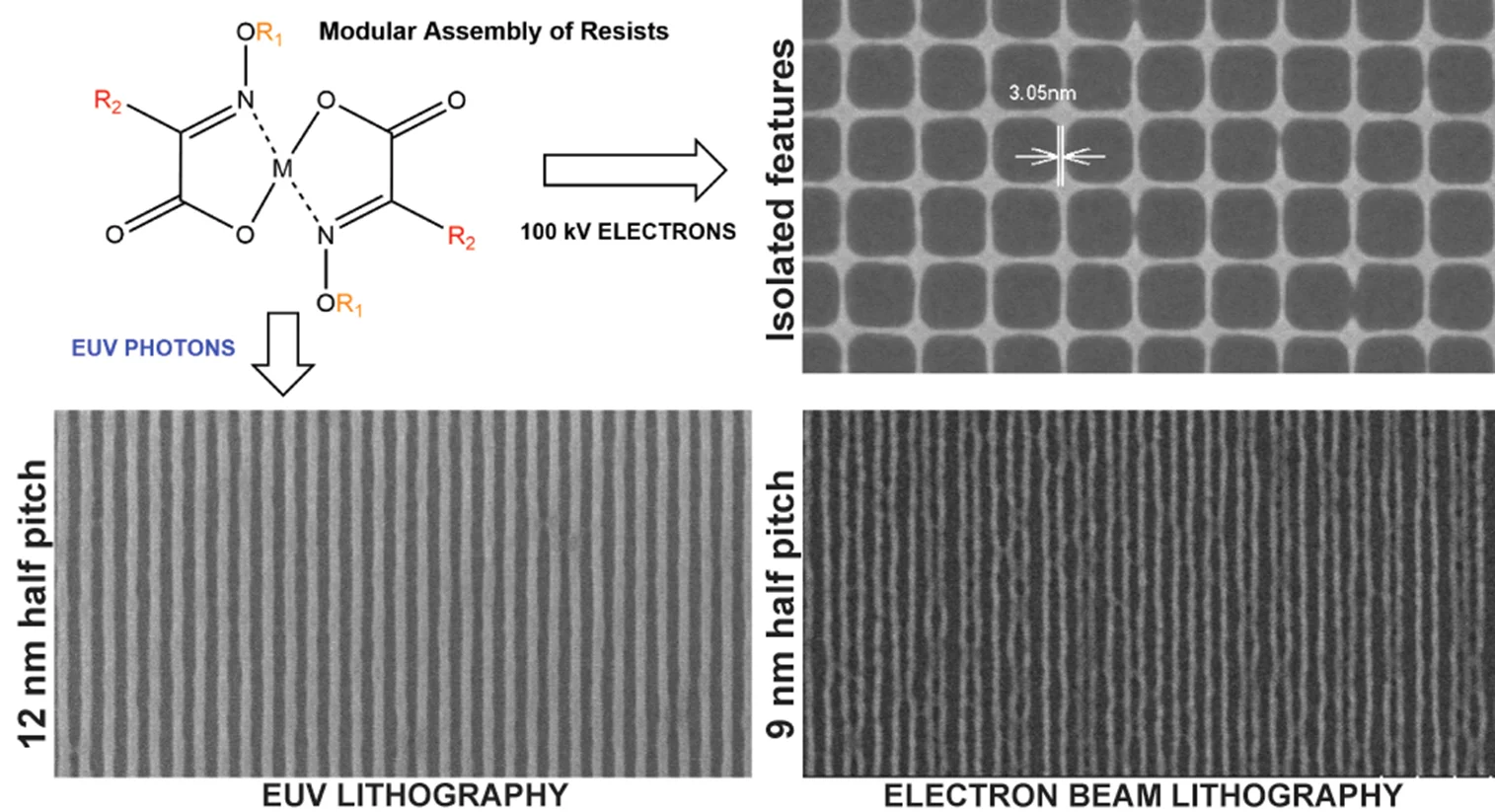
Photoresist materials are crucial in the manufacturing of computer chips, where the circuits are initially printed in the photoresist using photolithography. As the demand for smaller and more precise circuitry in computer chips grows, photoresists must resolve features with smaller sizes and higher density. One of the factors determining the ultimate resolution in lithography is the molecular size/mass of the photoresists. However, lower molecular mass materials are notoriously difficult to translate into photoresists due to their limited solubility in organic solvents and tendency to crystallize rather than to form smooth films on silicon wafers. A team of scientists from the Paul Scherrer Institut (Switzerland), the Brookhaven National Labs (USA), and institutes in Singapore have overcome this problem by reducing the resist to just two components: a metal atom and a radical initiator bonded to it. These two components can be changed or modified in a modular fashion, akin to assembling LEGO bricks. This versatile low molecular mass resist platform is compatible with electron beam lithography as well as extreme ultraviolet (EUV) lithography. This paradigm shift in resist chemistry has led to lithographic features approaching angstrom scale with very low linewidth roughness. Using small molecular size resists, a record 1.9−2.0 nm isolated patterns and 7 nm half-pitch dense line-space features are demonstrated. The researchers think that ultimate resolution is limited by instrumental factors and potential patterning at the level of a unit cell can be envisaged, paving the way towards angstrom-scale lithography. These findings have been published in ACS Nano.


