Sputtering is an all-purpose technology for producing thin layers and layer systems. Gas ions out of a plasma are accelerated towards a target consisting of the material to be deposited. As shown in fig.1, material is detached ("sputtered") from the target and deposited on a substrate.
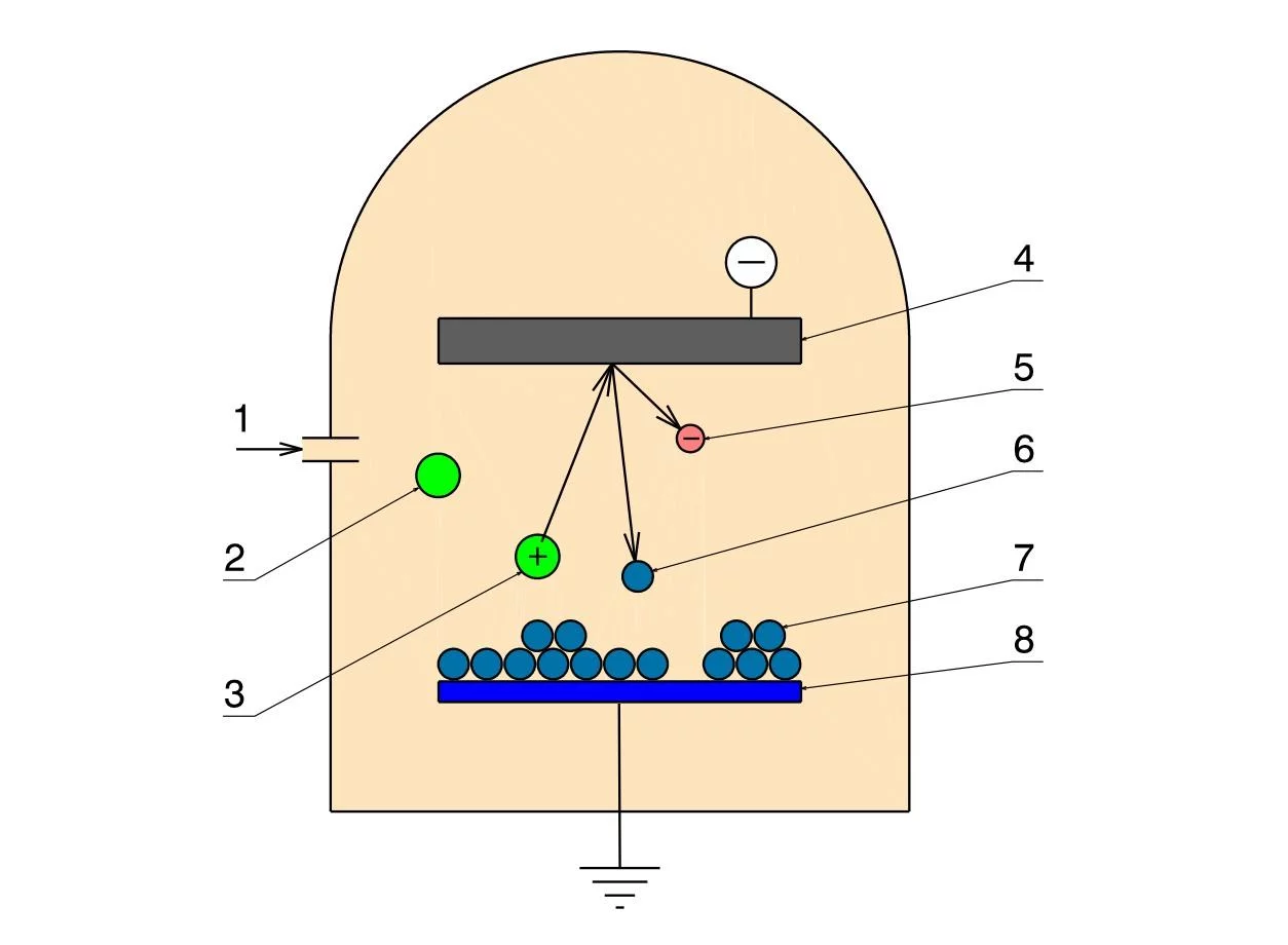
1 gas inlet to vacuum chamber
2 Ar-atom
3 ionisazion by electron impact
4 target on a negative potential
5 secondary electron
6 sputtered target atom
7 growing layer
8 substrate
2 Ar-atom
3 ionisazion by electron impact
4 target on a negative potential
5 secondary electron
6 sputtered target atom
7 growing layer
8 substrate
Three different targets can be used alternately to deposit target material. It is possible to coat films with a thickness from 1nm up to 1000nm. The area for a homogeneous coating is 50x200mm in the in-house built sputtering machine TIPSI (picture 1) whereas in the sputtering plant Leybold Z600 an area of 400x580mm is possible to coat, (picture 2).
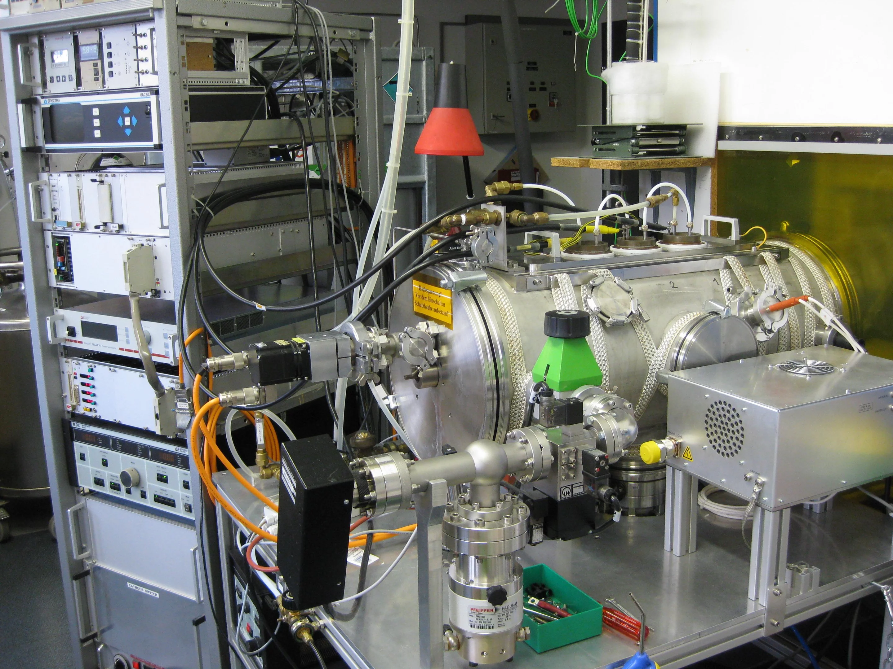
TIPSI
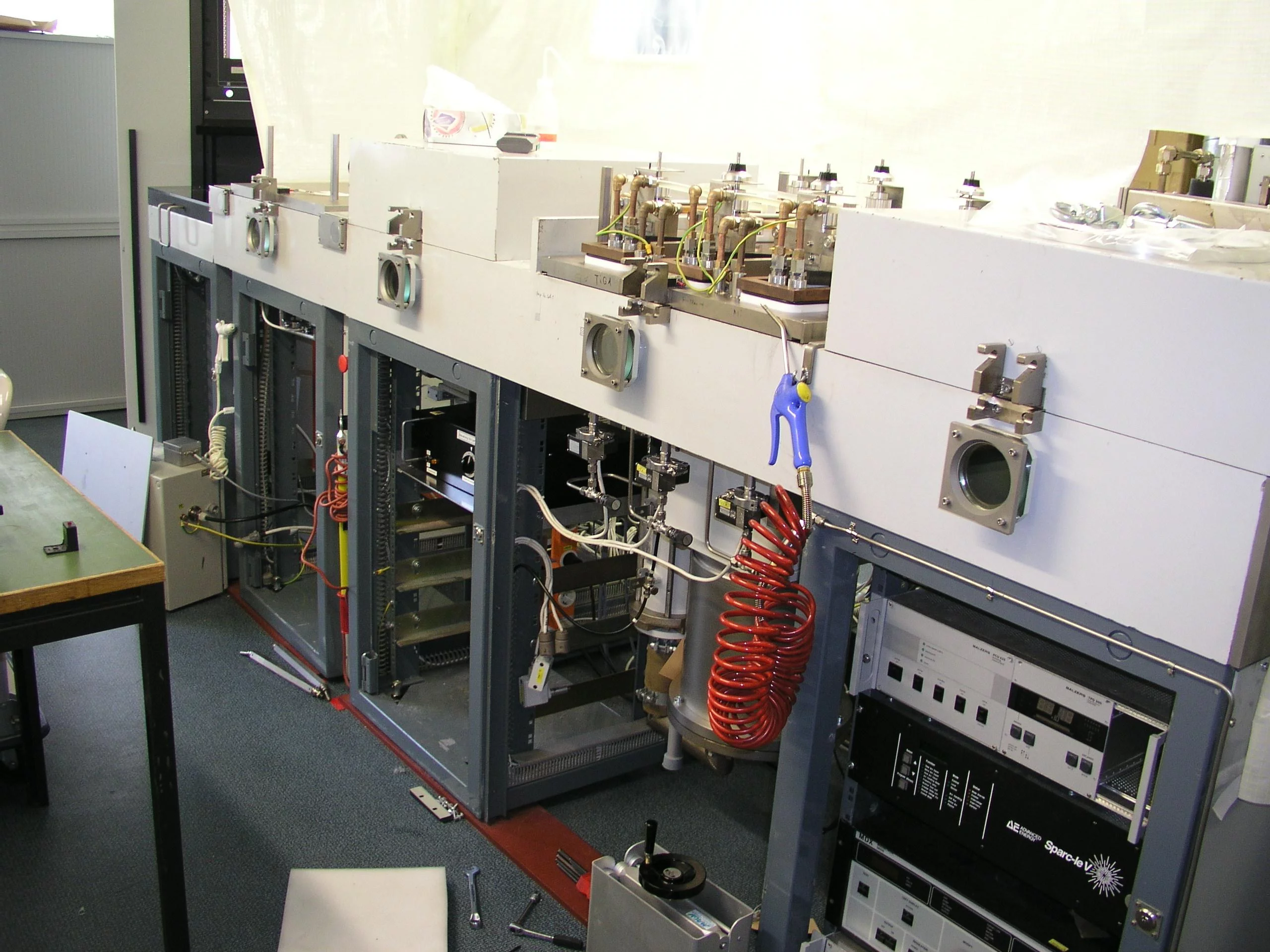
Leybold Z600
We are producing successfully Ni/Ti supermirrors up to m=5 and polarising remanent FeCoV/Ti:N mirrors up to m=3 for neutron optical applications and multilayer systems for X-ray deflection. A broad variety of layer coatings is possible. The available target material consists of more than 25 different materials. Many PSI groups profit from this possibility preparing their samples for experiments.
We offer our know how in sputtering techniques to other research institutions and to industrial companies. See below a list of actual external customers.
- Several private companies
- ETH Zürich, Inst. f. Biomedizinische Technik, Gloriastrasse 35, CH-8092 Zürich
- ETH Zürich, Professur für Oberflächentechnik, Wolfgang-Pauli-Str. 10, CH-8093 Zürich
- EMPA, Lab.for Joining Technologies&Corrosion, Ueberlandstrasse 129, CH-8600 Dübendorf