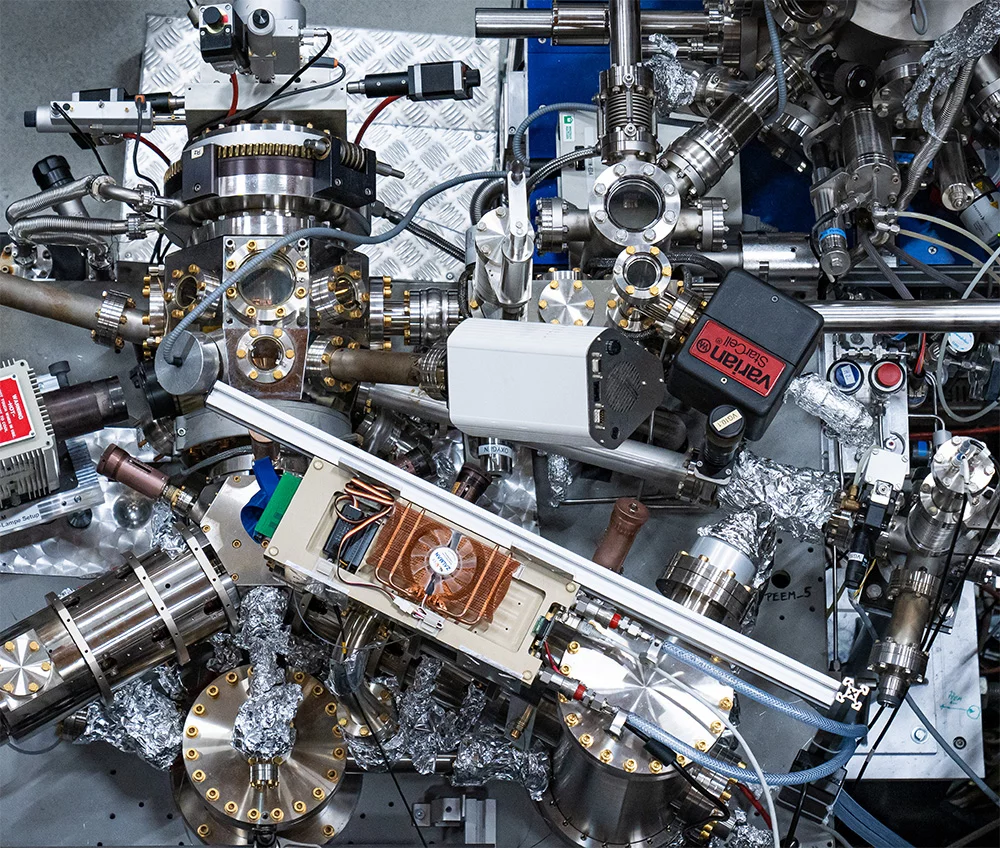
Endstation ES1: Photoemission electron microscope
| Spatial resolution | down to ~50 nm depending on sample |
|---|---|
| Electron energy resolution | 0.2 eV |
| Sample temperature | 120 K < T < 1'800 K |
| Field of view | 5 - 150 μm diameter |
The permanent endstation of the SIM beamline is a Photoemission Electron microscope (PEEM) (Model: LEEM III, Elmitec GmbH). It allows one to image samples using the photoelectric effect with very high spatial resolution. With an additional energy analyzer these photoelectrons are then energy-selected. In addition to illumination by X-rays, illumination by low energy electrons is possible. In this low energy electron microscopy (LEEM) mode, additional contrast mechanisms are available. For more information on PEEM for example lookup the web page of the LEEM User Community. The PEEM is equipped with a small preparation chamber (sputtering, heating, load-lock), while a larger preparation system equipped with LEED and e-beam evaporators, is also available.
When the sample is retracted, the light passes through the PEEM and can be used in a second endstation supplied by the user. Here an unfocussed beam of about 1 x 3 mm2 is available.
When the sample is retracted, the light passes through the PEEM and can be used in a second endstation supplied by the user. Here an unfocussed beam of about 1 x 3 mm2 is available.
Sample conditions
PEEM is a surface sensitive technique. Its depth of view is limited by the inelastic mean free path of the photoelectrons which is typically ~5 nm. The PEEM operates in UHV and with a high acceleration voltage (Va = 10-20 kV) to accelerate the inelastically scattered photoelectrons into the microscope lenses to produce a magnified image of the intensity of the locally emitted photoelectrons.For successful imaging in the PEEM the sample should meet the following conditions:
- sample dimensions: diameter < 10 mm, thickness ~0.1-3 mm
- UHV compatible (p < 10-8 mbar)
- flat and conducting surfaces are likely to produce high quality images with good spatial resolution.
Endstation ES3: X-ray Magnetic Circular Dichroism
| Scientific applications | Spectroscopy of ferromagnetic and antiferromagnetic materials |
|---|---|
| Experimental techniques | XAS, XMCD, XMLD |
| Characteristics | UHV chamber with external electromagnet |
| Detectors | Sample current with high voltage bias |
| Spot size at the sample | ~0.3 mm x 1.5 mm (H x V) |
| Sample requirements | Solid samples, up to 10 x 10 mm2 (surface area) and max. thickness of 1 mm. |
| Sample preparation | None |
| Sample environment | UHV Temperature range: 20 K to 600 K Temperature controlled heating |
| Magnetic field | Dipolar electromagnet: ± 130 mT Magnetic field/hellicity switching within 1-2 s. Possibility to do time-resolved polarization measurements. |
