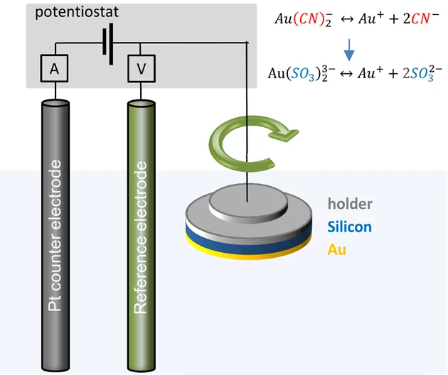
We recently modified the existing electroplating set up to a considerably faster, cleaner and, safer method by moving from a cyanide based Au electrolyte (commonly used) to a sulfite based Au electrolyte. Strict control of the deposition parameters is possible by using a 3-electrode configuration in conjunction with a potentiostat. The potentiostat applies a variable potential difference between the sample to be plated (working electrode) and the Pt or Au wire (the counter electrode), using a mercury sulfate electrode as the potential reference (reference electrode). In addition to rotating the sample in the plating solution, this process enables faster deposition rates and controllable growth modes in the presence of different p-block metal additives.
One such example is bottom-up Au filling of high aspect ratio silicon for use in grating-based X-ray technologies. Typically, in high aspect ratio/recessed features, sidewall growth can lead to early closing of the features to be filled resulting in voids – typically detrimental with respect to X-ray optics applications. The same is true for conformal growth in very deep structures, with the added disadvantage that conformal growth above the recessed features would lead to overfilling/waste and may require additional processing steps such as etching. With strict control of the deposition parameters as previously explained, bottom-up accelerated growth (Au deposition) can be realised. Resulting in, fully-filled, dense structures, free of any voids and with minimal deposition on the top of the field controllable by potential and the rotation rate.
Apart from bottom-up Au electroplating, the TOMCAT group is also involved in Au pulsed electrodeposition and Pd electroless deposition. Non electrochemical techniques have been also developed such as Ir atomic layer deposition and metal casting of Au-Sn and Pb based alloys.
Publications
- Jefimovs K, et al. Fabrication of X-ray Gratings for Interferometric Imaging by Conformal Seedless Gold Electroplating. Micromachines 12, 517 (2021).
- Josell D, Shi Z, Jefimovs K, Romano L, Vila-Comamala J, Moffat TP. Pushing the Limits of Bottom-Up Gold Filling for X-ray Grating Interferometry. J Electrochem Soc 167, 132504 (2020).
- Josell D, et al. Bottom-Up Gold Filling in New Geometries and Yet Higher Aspect Ratio Gratings for Hard X-ray Interferometry. J Electrochem Soc 168, 082508 (2021).
- Romano, L. et al. High aspect ratio metal microcasting by hot embossing for X-ray optics fabrication. Microelectronic Engineering 176, 6-10 (2017).
- Romano, L., Vila-Comamala, J., Schift, H., Stampanoni, M. & Jefimovs, K. Hot embossing of Au- and Pb-based alloys for x-ray grating fabrication. Journal of Vacuum Science & Technology B, Nanotechnology and Microelectronics: Materials, Processing, Measurement, and Phenomena 35, 06G302 (2017).
Collaboration
- Mr. Zhitian Shi, Dr. Konstantins Jefimovs, Dr. Lucia Romano, Paul Scherrer Institute, 5232 Villigen, Switzerland
- Dr. Martin Stauber, GratXray, PARK innovAARE, 5234 Villigen, Switzerland
- Dr. Daniel Josell, NIST, Gaithersburg, Maryland 20899, USA
Funding
- ETH, PSI, GratXray, SwissLos Kanton Aargau
Contact
Dr. Lucia Romano, lucia.romano@psi.ch, +41 56 310 56 88
Dr. Craig Lawley, craig.lawley@psi.ch, +41 56 310 2922