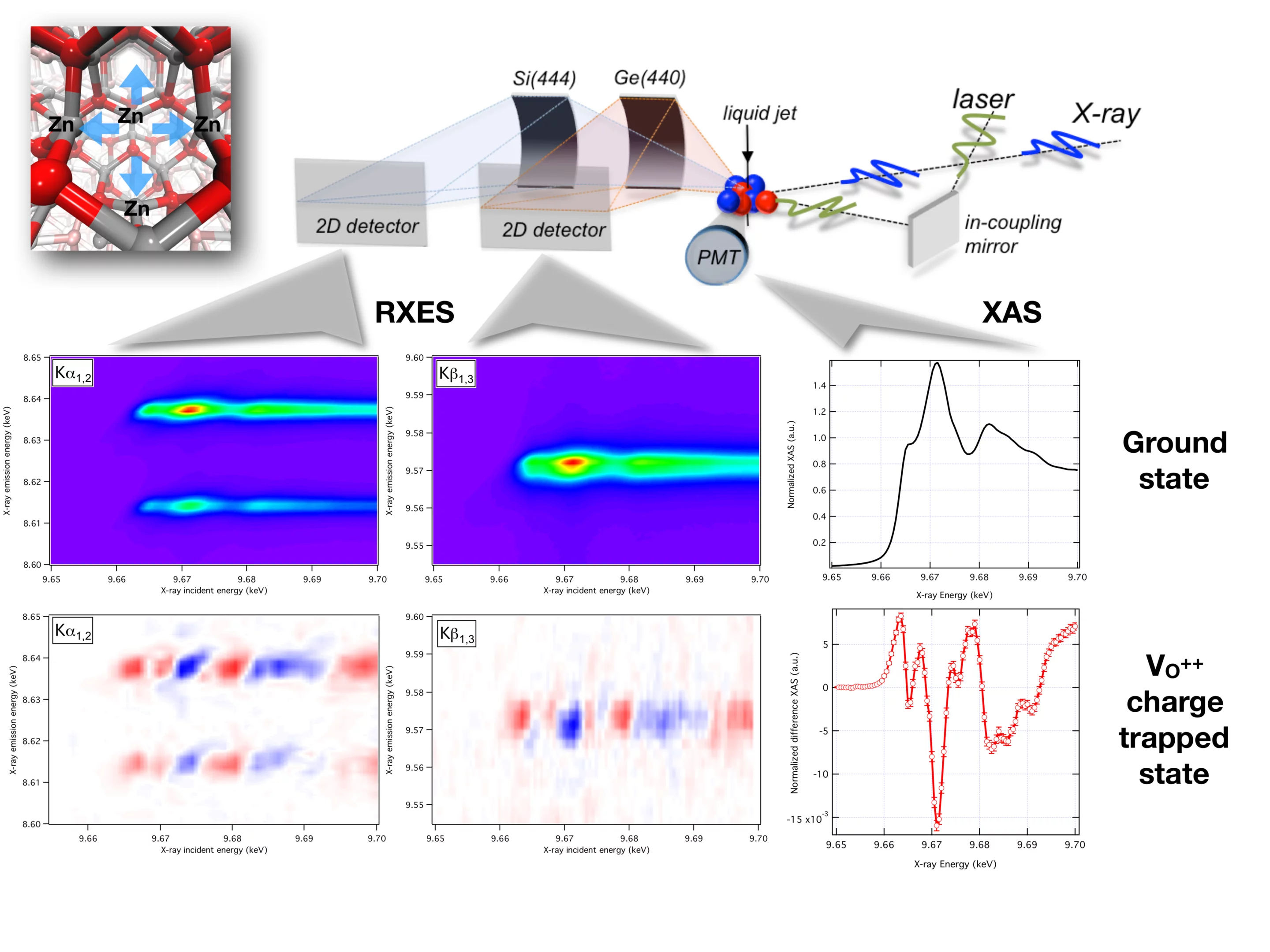
Members of the Alvra group led an investigation into the fate of charge carrier dynamics in metal oxide semiconductor nanomaterials. The experiments were performed at the Advanced Photon Source (Argonne, IL, USA) and used a PSI-designed von Hamos geometry X-ray emission spectrometer that was constructed for the experiment to perform resonant XES measurements on a solution of 32 nm diameter ZnO nanoparticles photo-excited with 3.2 eV (355 nm) short laser pulses. The measurement showed that the hole-trapping takes place within less than 100 ps and the trapping site in the ZnO crystal lattice is at oxygen vacancies in the lattice. The trapping of the hole results in a local structural distortion, where the four neighbouring Zn atoms move away from the vacancy. The measurement demonstrated the strength of the RXES technique's ability to probe both the electronic and geometric structure of materials and the results were recently published in Nature Communications. The experiment was a collaboration between members of Argonne National Labs, European XFEL GmbH, EPFL, and the Paul Scherrer Institute.
Contact person: Chris Milne (chris.milne@psi.ch)