Coherent Electron Source
The highly brilliant electron beam produced by field emitters is one of the enabling factors of the high resolution electron microscope with atomic resolution. In addition to high beam brightness, field emitters are also high current, high current density, and highly coherent cathodes. These characteristics motivated the use of field emitters for high-frequency vacuum electric tubes and accelerator applications and in experiments including electron diffraction, holography, coherent diffraction imaging, to name a few.
An important, yet to be elucidated property of field emission beam is the propagation of the spatial coherence; field emission electrons are produced by quantum mechanical tunneling through the surface barrier from the solid. As such, the wave function of the field emission electrons are dictated by the momentum distribution of electrons in the solid, which appears to limit the minimal transverse source size of a field emitter [1] and the minimal coherent fraction of the field emission beam [2]. By analyzing these characteristics, we concluded that the field emission beam propagation and the transverse emittance are limited by the average transverse energy spread [1,2,3], as calculated by the standard field emission theory [4]. Recent experiments on the measurement of the transverse emittance of molybdenum double-gate nanotip field emitter arrays (FEAs) [3] and the beam propagation of single-molybdenum-nanotip double-gate field emitters demonstrated that the transverse emittance and the minimal beam spread at the maximally collimated field emission beam are dictated by the average transverse energy spread.
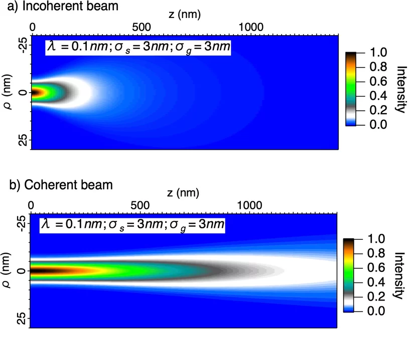
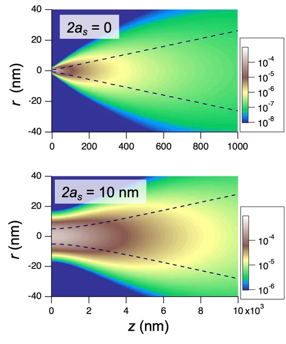
The analysis [2] of the field emission beam showed that our single-molybdenum-nanotip with the tip-apex-size of 5-10 nm should exhibit the coherence fraction of 10-20% because of the minimal size of field emission beam equal to ~1 nm as determined by the uncertainty principle and the average transverse energy spread of ~0.1 eV. When the propagation of such field emission beam is analyzed by theory of partially coherent beam [5], which predicts the conservation of the coherence fraction upon propagation, substantial spatial coherence, reaching microns without any additional aperture stop, is predicted [2]. This is in strong contrast to the analysis by van Cittert Zernike theorem with the orders of magnitude smaller (but still amounts to tens of nanometers) transverse coherence length. So far, the precision for the transverse coherent length measurement based on an experiment based on the low energy electron diffraction [6] is not sufficient to distinguish the two theory, i.e. if a field emitter is an incoherent cathode or a (partially) coherent cathode on the cathode surface. Figure 1 shows that when the beam spread of a field emission beam is substantially narrower when the spatial coherence at the source is finite [2]. Furthermore, when the field emission beam is completely coherent, the finite source size makes the beam spread even narrower as depicted in Figure 2 [1]. Since the elucidation of the spatial coherence is relevant to the electron microscope based on the coherent scattering and computational reconstruction, this is a subject of active research.
Referernces
[1] S. Tsujino, Transverse structure of the wave function of field emission electron beam determined by intrinsic transverse energy, J. Appl. Phys. 124, 044304 (2018). https://doi.org/10.1063/1.5035284,
[2] S. Tsujion, On the brightness, transverse emittance, and transverse coherence of field emission beam, Journal of Vacuum Science & Technology B 40, 030801 (2022) (featured article); https://doi.org/10.1116/6.0001776.
[3] S. Tsujino, P. D. Kanungo, M. Monshipouri, C. Lee, and R. J. D. Miller, Measurement of transverse emittance and coherence of double-gate field emitter array cathodes, Nat. Commun. 7, 13976 (2016); https://doi.org/10.1038/ncomms13976.
[4] CR. H. Good and E. W. Müller, “Field emission,” in Electron-Emission Gas Discharges I/Elektronen-Emission Gasentladungen I (Springer, Berlin, 1956), pp. 176–231.
[5] C. Lee, P. D. Kanungo, V. A. Guzenko, P. Hefenstein, R. J. D. Miller, and S. Tsujino, Field emission beam characteristics of single metal nanotip cathodes with on-chip collimation gate electrode, J. Vac. Sci. Technol. B 33, 03C111 (2015);https://doi.org/10.1116/1.4913397.
[6] C. Lee, S. Tsujino, and R. J. D. Miller, Transmission low-energy electron diffraction using double-gated single nanotip field emitter, Appl. Phys. Lett. 113, 013505 (2018);https://doi.org/10.1063/1.5030889.
Electron wavefront engineering
The purpose of this project is to manipulate the wave front of coherent free electron wave functions to realize a novel electron diffraction imaging method. Spatial phase modulators that synthesize arbitrarily pulse shapes in space and time are available for coherent electromagnetic waves but coherent manipulation of electron beam is much less explored. For example, the direct demonstration of the quantum mechanical nature of free electrons via Young’s double‐slit interference experiment as described by R. P. Feynman [7] was reported only recently [8,9], even though the electron wave interference has been demonstrated more than 50 years ago [10].
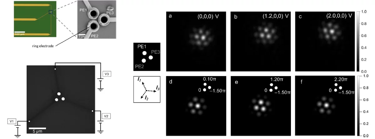
A Boersch phase plate can shift the phase of electrons proportionally to the applied electrical potential, thereby allowing for in situ control of the electron phase shift. A device comprising multiple Boersch phase shifter elements will be able to modulate the wavefront of a coherent electron beam and control electron interference. In a recently published work [11], we developed a fabrication method utilizing the state-of-the-art electron beam lithography and reactive ion etching processes, a combination that is widely used for high-throughput and large-scale micro- and nanofabrication of electronic and photonic devices. Using the developed method, we fabricated a three-element phase shifter device with a metal–insulator–metal structure with 100-nm-thick ring electrodes and tested its electron transmission characteristics in a transmission electron microscope with a beam energy of 200 keV. We observed voltage-controlled evolution of electron interference, demonstrating the voltage-controlled electron phase shift using the fabricated device with a phase shift of π rad per 1 V, see Figure 3. We analyze the experimental results in comparison with a three-dimensional electrostatic simulation.
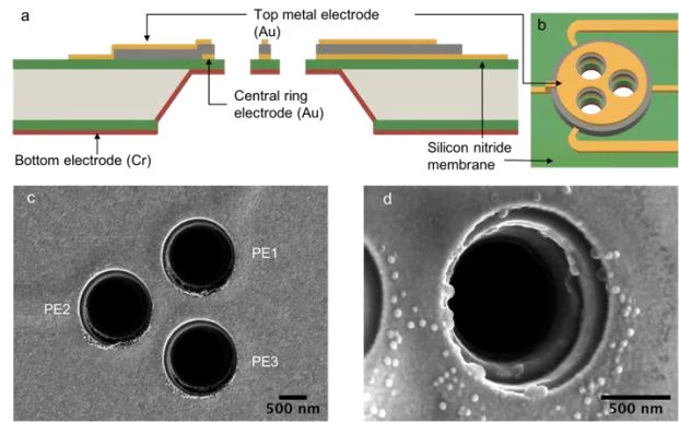
In a recent follow up work, we have successfully fabricate a five-layer device structure and tested its phase shift characteristics. We have found that the beam deflection and crosstalk between phase shifter elements are substantially reduced [12], see Figure 4. The work demonstrates the possible up-scaling of the array device with orders of magnitude more phase elements.
Referernces
[7] R. P. Feynman, R. B. Leighton, M. Sands, The Feynman Lectures on Physics (Addition‐Wesley, Menlo Park, CA, 1965), Vol. III. III, Ch. 1, section 1‐5.
[8] S. Frabboni, G. C. Gazzadi, G. Pozzi, Young’s double‐slit interference experiment with electrons, Am. J. Phys. 75, 1053 (2007).
[9] R. Bach, D. Pope, S.‐H. Liou, H. Batelaan, Controlled double‐slit electron diffraction, New J. Physics 15, 033018 (2013).
[10] C. Joensson, Elektroneninterferenzen an mehreren kuenstlich hergestellten Feinspalten, Z. Physik 161, 454 (1961).
[11] P. Thakkar, V. A. Guzenko, P.-H. Lu, R. E. Dunin-Borkowski, J. P. Abrahams, S. Tsujino, Fabrication of low aspect ratio three-element Boersch phase shifters for voltage-controlled three electron beam interference, J. Appl. Phys. 128, 134502 (2020); https://doi.org/10.1063/5.0020383.
[12] P. Thakkar, V. A. Guzenko, P.-H. Lu, R. E. Dunin-Borkowski, J. P. Abrahams, S. Tsujino, Voltage-controlled three-electron-beam interference by a three-element Boersch phase shifter with top and bottom shielding electrodes, 34th International Vacuum Nanoelectronics Conference (Lyon, France, 2021); https://doi.org/10.1109/IVNC52431.2021.9600711.
