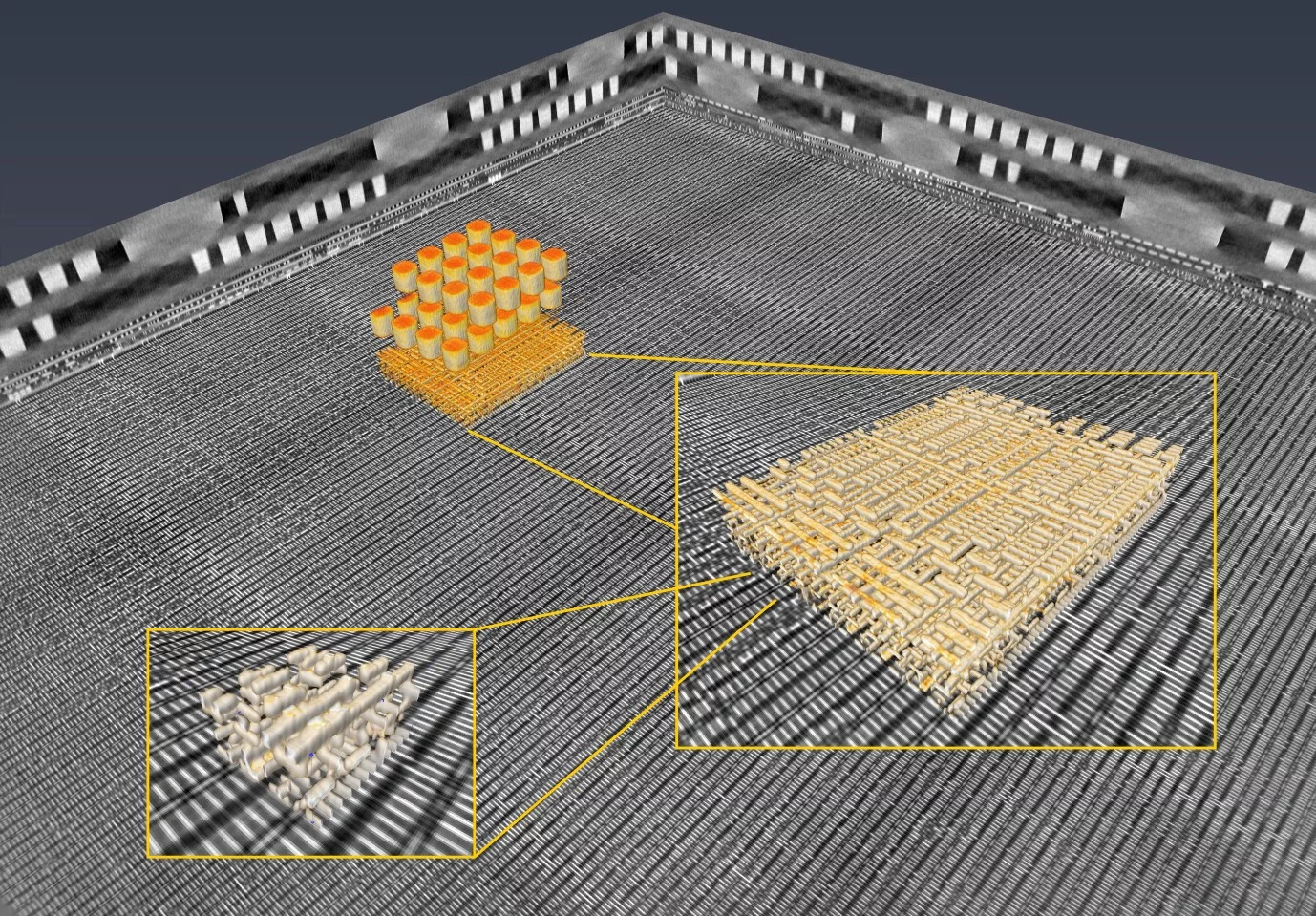
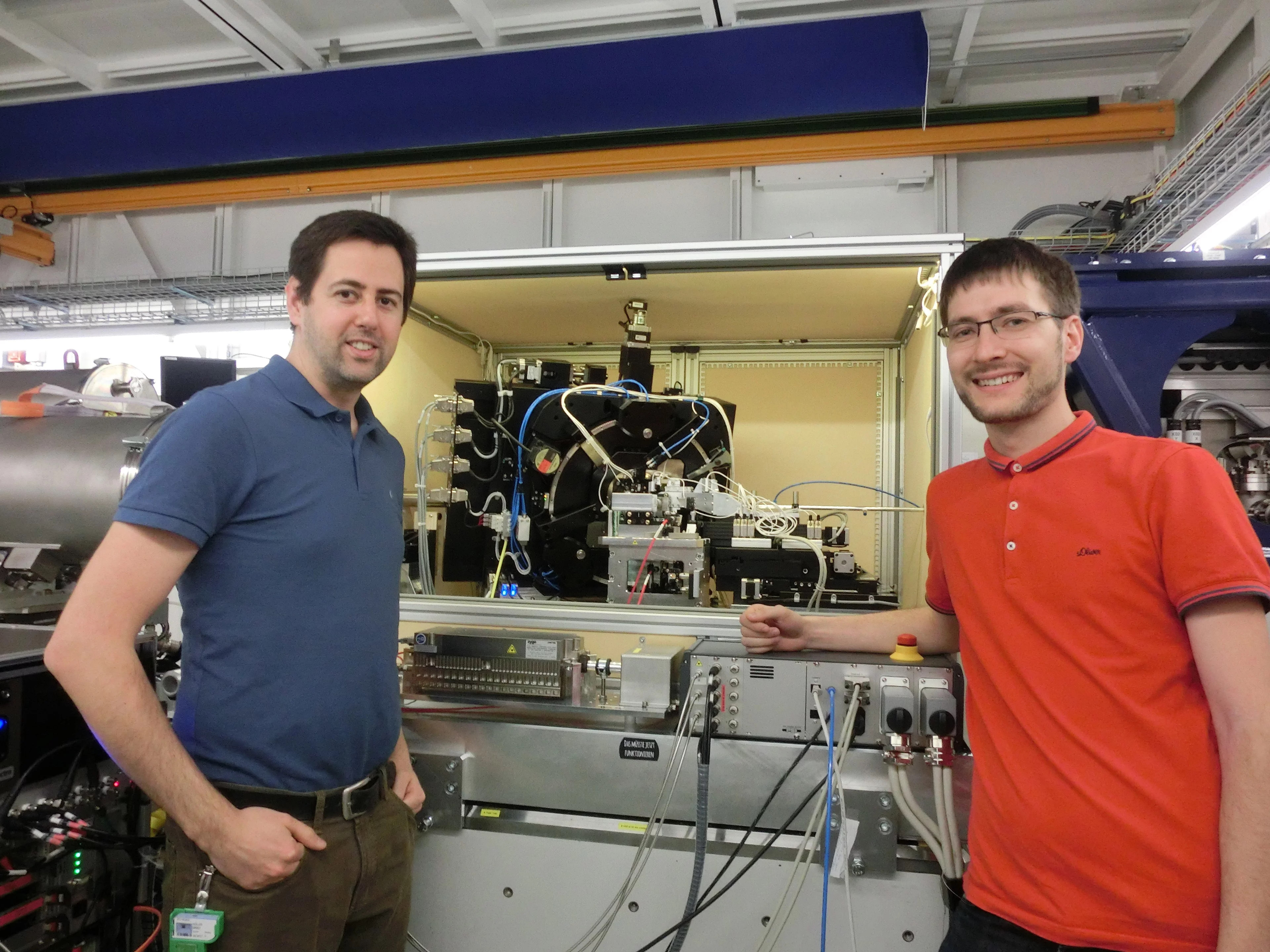
Researchers of the Paul Scherrer Institut have previously generated 3-D images of a commercially available computer chip. This was achieved using a high-resolution tomography method developed over several years. However, such non-destructive tomography imaging requires tedious sample preparation of small volumes to be extracted from the planar integrated circuit. Now they extended their imaging approach to a so-called laminography geometry to remove the requirement of preparing isolated samples, also enabling imaging at various magnification. For ptychographic X-ray laminography (PyXL) a new instrument was developed and built, and new data reconstruction algorithms were implemented to align the projections and reconstruct a 3D dataset. The new capabilities were demonstrated by imaging of a 16 nm FinFET integrated circuit. A full chip was mounted in the instrument and first a low resolution overview scan covering a large region of 300 x 300 µm2 was imaged and allowed the selection of a smaller region of interest. This part covering a field of view of 40 µm diameter was imaged at 18.9 nm 3D resolution without any further sample preparation in the same instrument. The researchers conducted the experiments at the Swiss Light Source SLS of the Paul Scherrer Institut and report these results in the latest edition of the journal Nature Electronics. The imaging technique is not limited to integrated circuits, but can be used for high-resolution 3D imaging of flat extended samples. Thus the researchers start now to exploit other areas of science ranging from biology to magnetism.
Electron microscopy can reach unmatched resolution, but is either mostly surface sensitive in scanning electron microscopy (EM), or can only penetrate thin samples, on the order of a few hundred nanometers, in transmission EM. In contrast, X-rays of photon energy of a few keV can penetrate much thicker samples. The wavelength of such radiation is small enough that nanometric resolution is in principle possible. However, this high penetration, which comes from weaker interaction with matter, also makes it challenging to fabricate high numerical aperture lenses. In X-ray microscopes the imaging optics often sets the limit of resolution. The ability to probe deeper into volumetric structures, and measure larger and more representative volumes, provides an important complementarity to electron microscopy.
At the Paul Scherrer Institut Ptychographic X-ray computed tomography (PXCT), an extension to 3D of Ptychography, was pioneered. Ptychography is a lens-less imaging technique that combines scanning microscopy and coherent diffractive imaging: A sample is illuminated by a confined and coherent X-ray beam and far-field diffraction patterns are recorded at many regions of the sample with overlapped illumination [1]. The imaging system is replaced by an iterative reconstruction algorithm, which solves the phase problem and reconstructs a real-space image of the sample. The achievable resolution is therewith neither limited by the beam size, nor by the step size, but determined by the effective numerical aperture of the intensity detector array, the signal-to-noise ratio of the measured intensities, and the positioning accuracy of the scanning instrument.
After the first demonstration of PXCT [2] the development dedicated instrumentation for the technique began. A special laser interferometry ensures sample scanning with nanometric accuracy. Continuous improvement of such instrumentation allowed demonstrating high-resolution imaging of integrated circuits in 2017 [3], resolving all circuit connections in all layers of the chip down to the transistors in Intel’s 22 nm FinFET technology. A caveat of PXCT is that a small sample has to be extracted from the chip and mounted isolated, such that it is accessible to the radiation from all sides. This means that, although the X-ray measurement is non-destructive, the sample preparation is destructive, removes the sample region from the surroundings, and the measurement position must be selected prior the X-ray measurement. That is a clear limitation for many samples whose native state is within a flat extended surface.
A solution to this problem is to migrate to a laminography geometry, for which the axis of rotation is no longer perpendicular to the direction of X-ray propagation. First proposed in 1974 [4] and later implemented in conventional X-ray projection imaging [5], laminography would significantly simplify sample preparation and allow mounting full chips, but required a significant increase in imaging resolution. Ideally, various magnifications should be available to allow selecting a region of interest for a high-resolution measurement based on low-resolution data. Therefore the decision was made to combine laminography with X-ray ptychography, a technique now called PyXL (Ptychographic X-ray computed Laminography). As mentioned, nanometric sample positioning accuracy is required, and thus a dedicated instrument was developed and build at PSI, involving new ideas for the interferometic measurement of the sample position.
For the very first PyXL X-ray imaging test a full-sized chip for general-purpose logic manufactured in 16 nm FinFET technology, a sample that had been already characterized with electron microscopy and PXCT, was mounted. Low- and high-resolution laminograms were recorded. Novel codes for projection alignment and reconstruction, for generating a three-dimensional dataset from the collected projections were already written and only short time after the measurement the 3D dataset was available. The image quality allowed to resolving all chip layers and interconnects down to the lowest layer [6] as the resolution achieved in this first measurement was 18.9 nm.
The new method has proven to allow measuring flat samples at high resolution in 3D without the need to undergo a complex sample preparation. Moreover, various magnification levels are accessible within the same instrument. The resolution obtained is about an order of magnitude better compared to what was demonstrated in laminography before [7]. The method is not limited to integrated circuits but useful whenever a high-resolution image of a flat sample is needed, which has many useful applications for materials that don’t lend themselves well to be milled in pillars due to loss of structural integrity, and it simplifies significantly in situ or operando measurements.
[1] F. Pfeiffer, “X-ray ptychography,“ Nat. Photonics 12, 9–17 (2018)
[2] M. Dierolf, A. Menzel, P. Thibault, P. Schneider, C. M. Kewish, R. Wepf, O. Bunk, F. Pfeiffer, “Ptychographic X-ray computed tomography at the nanoscale,” Nature 467, 436–439 (2010)
[3] M. Holler, M. Guizar-Sicairos, E. H. R. Tsai, R. Dinapoli, E. Müller, O. Bunk, J. Raabe, G. Aeppli, “High-resolution non-destructive three-dimensional imaging of integrated circuits,” Nature 543, 402–406 (2017)
[4] F. A. Hasenkamp, “Radiographic Laminography”, Mater Eval 32, 169 (1974).
[5] L. Helfen, T. Baumbach, P. Mikulík, D. Kiel, P. Pernot, P. Cloetens, J. Baruchel, “High-resolution three-dimensional imaging of flat objects by synchrotron-radiation computed laminography,” Appl. Phys. Lett. 86 071915 (2005).
[6] M. Holler, M. Odstrcil, M. Guizar-Sicairos, M. Lebugle, E. Müller, S. Finizio, G. Tinti, C. David, J. Zusman, W. Unglaub, O. Bunk, J. Raabe, A. F. J. Levi, G. Aeppli, “Three-dimensional imaging of integrated circuits with macro to nanoscale zoom,” Nat. Electron. 2, DOI 10.1038/s41928-019-0309-z (2019)
[7] F. Xu, L. Helfen, H. Suhonen, D. Elgrabli, S. Bayat, P. Reischig, T. Baumbach, P. Cloetens, “Correlative Nanoscale 3D Imaging of Structure and Composition in Extended Objects,” PLoS One 7 e50124 (2012).
Contact
Dr. Mirko Holler
Paul Scherrer Institut
E-mail: mirko.holler@psi.ch
Original Publication
Mirko Holler, Michal Odstrcil, Manuel Guizar-Sicairos, Maxime Lebugle, Elisabeth Müller, Simone Finizio, Gemma Tinti, Christian David, Joshua Zusman, Walter Unglaub, Oliver Bunk, Jörg Raabe, A. F. J. Levi, and Gabriel Aeppli
Three-dimensional imaging of integrated circuits with macro- to nanoscale zoom.
Nature Electronics.
https://doi.org/10.1038/s41928-019-0309-z
Open SharediT link: https://rdcu.be/bTudW

