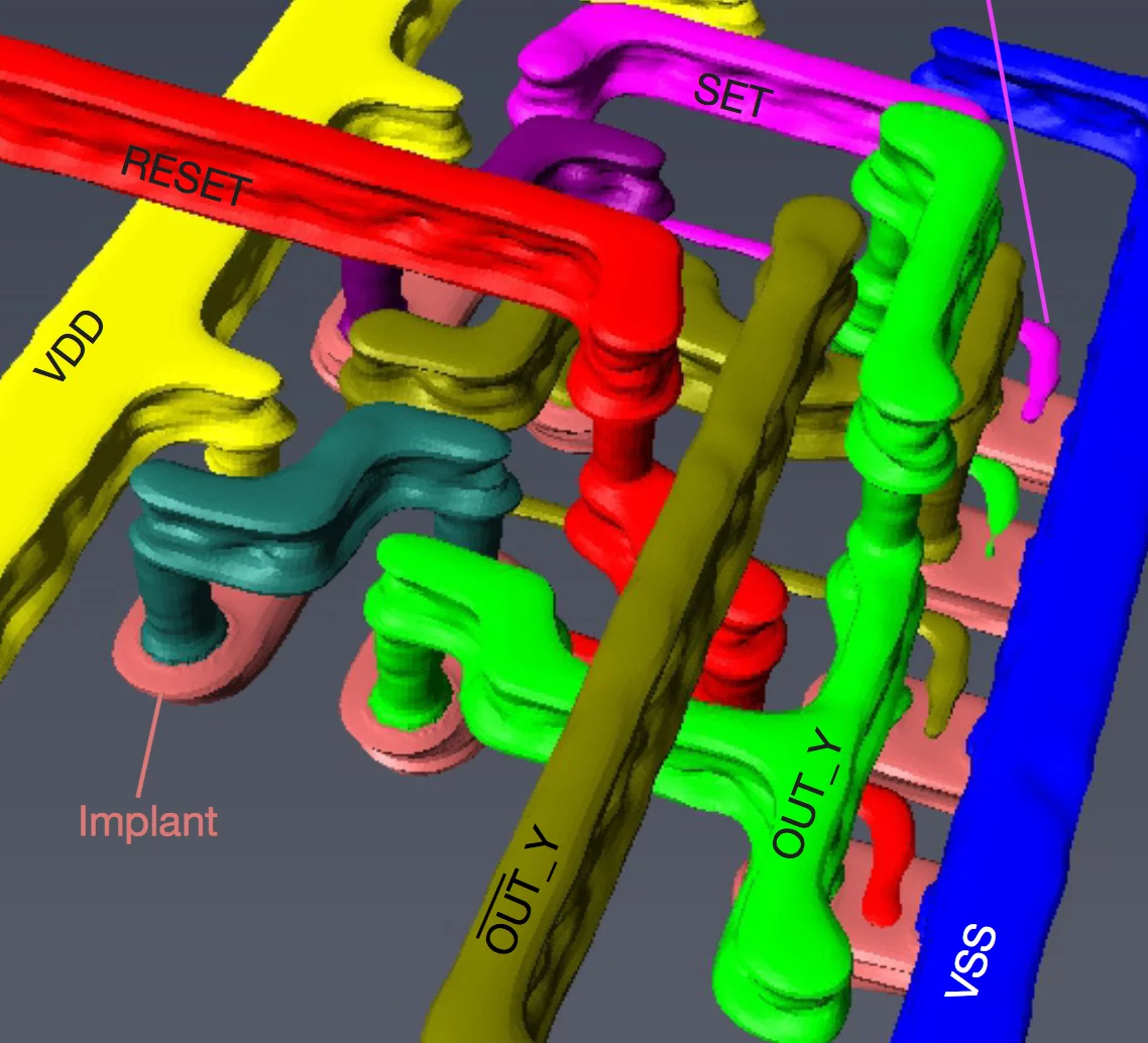
Modern nanoelectronics has advanced to a point at which it is impossible to image entire devices and their interconnections non- destructively because of their small feature sizes and the complex three-dimensional structures resulting from their integration on a chip. This metrology gap implies a lack of direct feedback between design and manufacturing processes, and hampers quality control during production, shipment and use. Here we demonstrate that X-ray ptychography - a high-resolution coherent diffractive imaging technique - can create three-dimensional images of integrated circuits of known and unknown designs with a lateral resolution in all directions down to 14.6 nanometres. We obtained detailed device geometries and corresponding elemental maps, and show how the devices are integrated with each other to form the chip. Our experiments represent a major advance in chip inspection and reverse engineering over the traditional destructive electron microscopy and ion milling techniques. Foreseeable developments in X-ray sources, optics and detectors, as well as adoption of an instrument geometry optimized for planar rather than cylindrical samples, could lead to a thousand-fold increase in efficiency, with concomitant reductions in scan times and voxel sizes.
- About the CentercloseAbout the Center
- Our Research
- Our User Facilities
- SINQ: Swiss Spallation Neutron Source
- SμS: Swiss Muon Source
- CHRISP: Swiss Research Infrastructure for Particle Physics
- Scientific Advisory Committees
- Publications
- Jobs & Education


