

Direct write e-beam lithography tools at LMN provide a variety of powerful techniques for the lateral as well as three-dimensional pattern transfer with the resolution down to 10 nm. Compared to other nanostructuring methods, it stands out for a high level of flexibility and reasonably high patterning speed.
Vistec EBPG 5000PlusES
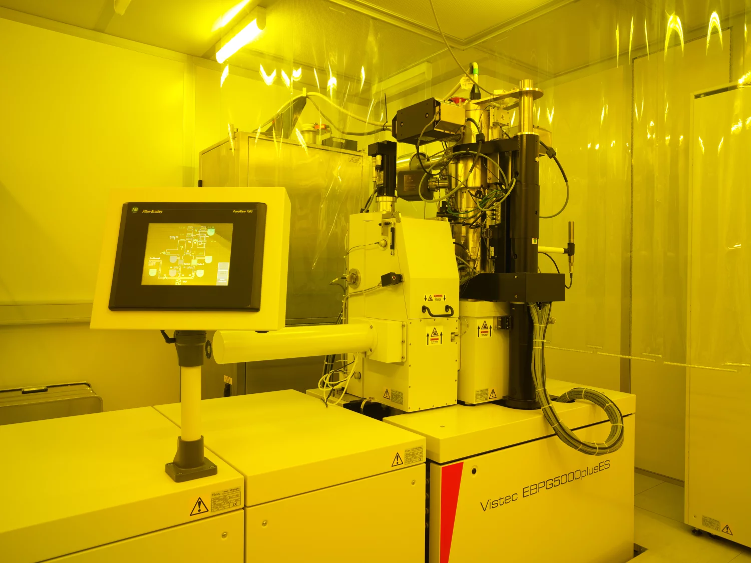
Vistec EBPG 5000PlusES installed in ODRA/55a
Vistec EBPG 5000Plus e-beam lithography tool is in operation since March 2009. It is installed in a dedicated cleanroom of class 100 with high precision temperature control at 21 ± 0.1° C. This is a prerequisite for the minimization of thermal drift in the electron optics, and thus, for the excellent performance of the system.
The main characteristics of the tool are:
- It is a vector-scan direct write tool with a Gaussian shaped beam. The beam scanning is controlled by combination of two deflection systems. Thus, the maximum writing field size of 512×512 µm² in conjunction with the beam stepping frequencies up to 50 MHz are achievable.
- The spot can be focused to less than 5 nm in diameter. Owing to the wide range of available beam currents (200 pA – 200 nA), the high-throughput as well as high-resolution exposures are possible.
- It is operated at 100 keV acceleration voltage. Up to several micrometers thick layers of e-beam resist can be exposed with small forward scattering.
- Wafers with diameter up to 150 mm and mask blanks up to 5×5 sq. inch can be processed.
- The overlay precision (mean + 3σ) is below 40 nm for the largest and 20 nm for smaller (100×100 µm²) write fields.
- For the conversion of the CAD patterns into machine specific format, including proximity effect correction (PEC), a special software solution – Layout BEAMER – is used. In some special cases, a direct coding of the beam movement is advantageous, which allows up to speed up remarkable the exposure or improve further the resolution.
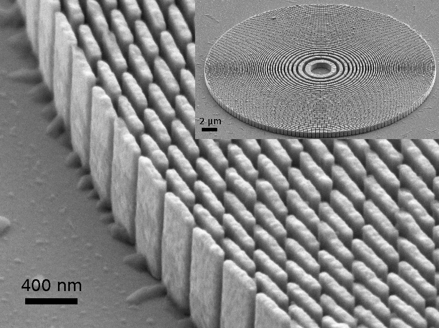
Fresnel zone plate (Gold, electroplating in PMMA mold)
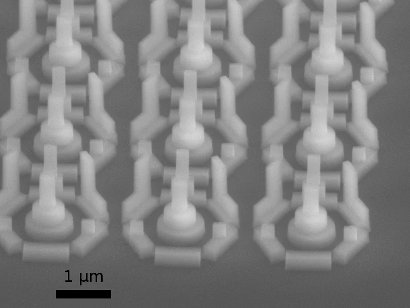
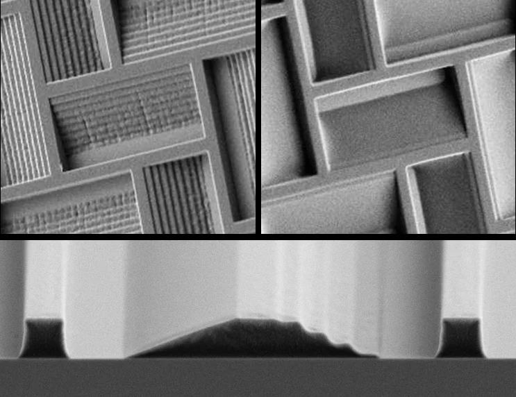
Multilayer HSQ structures (overlay exposures)
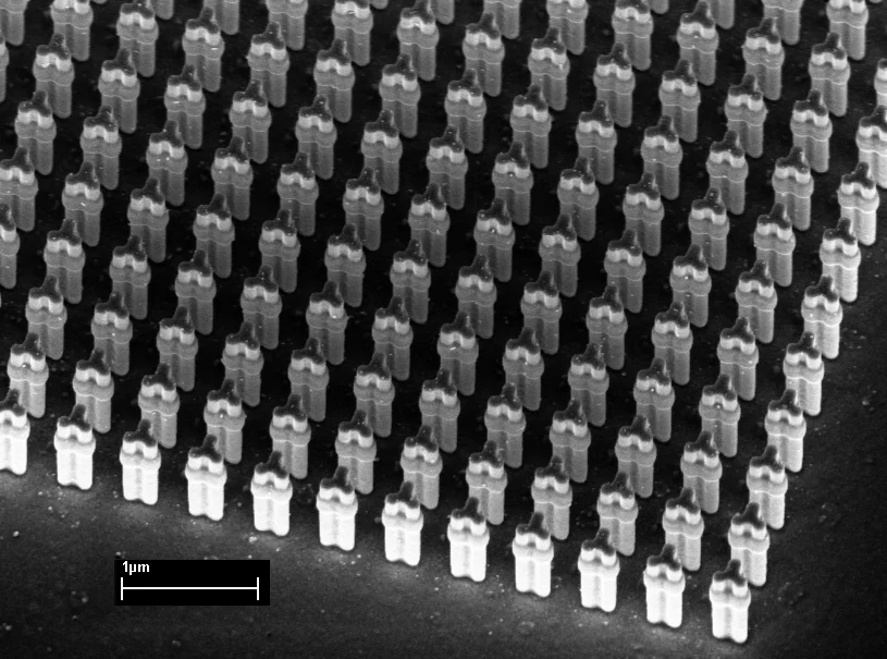
Artificial 2D crystal made of high aspect ratio structures (Gold, electroplating in a PMMA mold)
3D Topological profiles in 1 µm thick PMMA layer