

We have been studying all-metal field emitter array (FEA) cathode [1-14] as a potential high current and high brilliance electron source for advanced accelerator applications e.g. X-ray free electron lasers such as SwissFEL [15], requiring stringent cathode specs: high current (200 pC in 10 ps), low normalized transverse emittance (0.4 mm-mrad), and compatibility with the high acceleration electric field in the order of 100 MV/m.
For that, we have proposed the double-gate nanotip FEAs with surface-plasmon-enhanced laser-induced field emission: electrons from 1 million nanotips are produced by near infrared laser pulses, of which optical electric field is enhanced via the surface-plasmon-polariton resonance of the cupper-double-gate structure and the lightening rod effect at the molybdenum nanotip apexes.
The double-gate FEAs with the demonstrated collimation capability are expected to open up new electron beam applications including micro electron microscope, sub-THz and THz vacuum electronic power amplifiers, ultra-compact mass spectrometers, compact X-ray sources, parallel e-beam lithography tools, etc.
In collaboration with the University of Hamburg, we also conduct research directing to developing the brightest, next generation electron sources, for atomically resolving the structure-function correlation in biological systems to directly observe biology in action at atomic level.
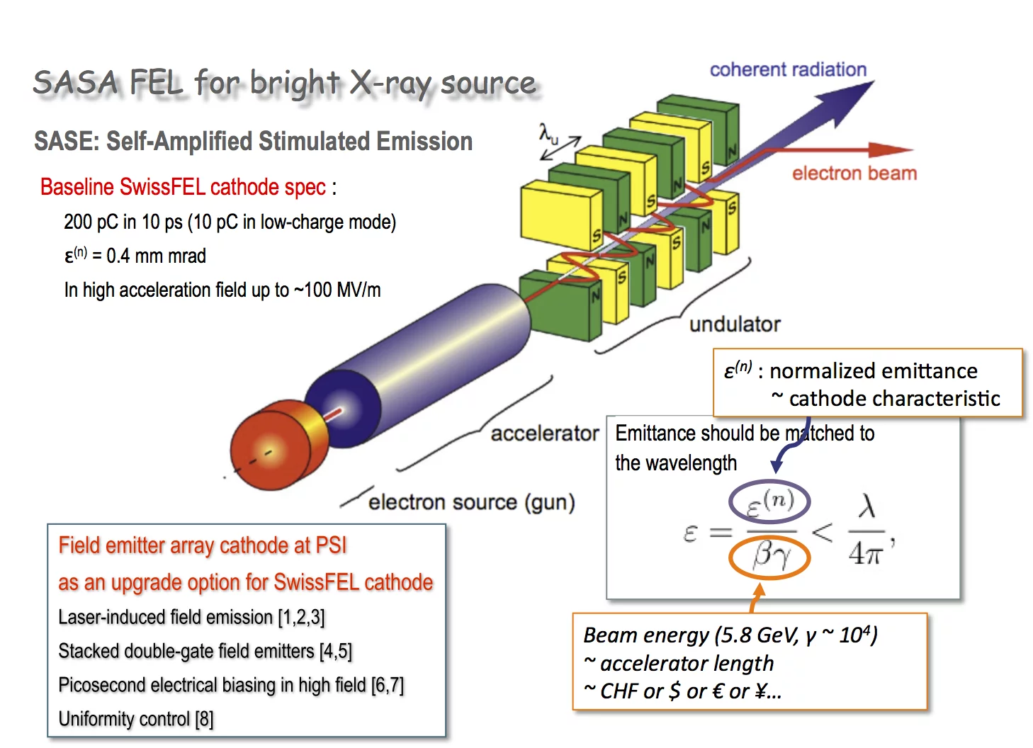
Fig.1 SASE X-ray free electron laser and low-emittance cathode
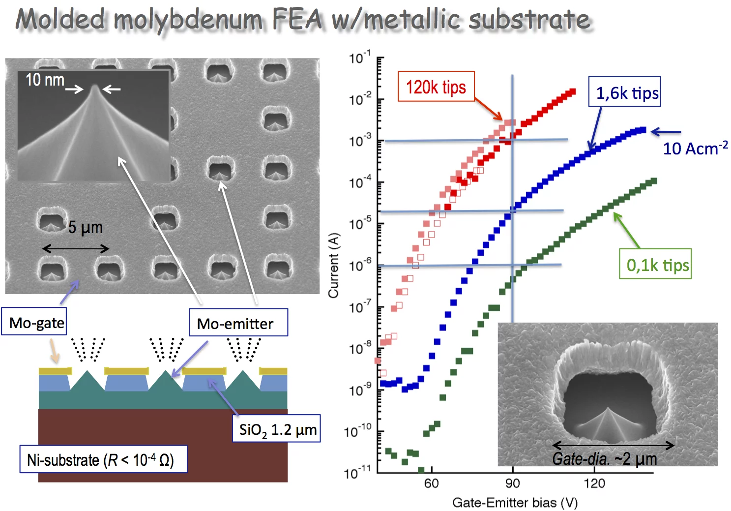
Fig.2 PSI Field-emitter array cathode: overview
References
[1] S. Tsujino, P. Beaud, E. Kirk, T. Vogel, H. Sehr, J. Gobrecht, and A. Wrulich, Ultrafast electron emission from metallic nanotip arrays induced by near infrared femtosecond laser pulses, Appl. Phys. Lett. 92, 193501 (2008).[2] S. Tsujino, F. le Pimpec, J. Raabe, M. Buess, M. Dehler, E. Kirk, J. Gobrecht, and A. Wrulich, Static and optical field enhancement in metallic nanotips studied by two-photon photoemission microscopy and spectroscopy excited by picosecond laser pulses, Appl. Phys. Lett. 94, 093508 (2009).
[3] A. Mustonen, P. Beaud, E. Kirk, T. Feurer, and S. Tsujino, Five picocoulomb electron bunch generation by ultrafast laser-induced field emission from metallic nano-tip arrays, Appl. Phys. Lett. 99, 103504 (2011).
[4] A. Mustonen, P. Beaud, E. Kirk, T. Feurer, and S. Tsujino, Efficient light coupling for optically excited high-density metallic nanotip arrays, Scientific Reports, 2, 915 (2012).
[5] S. Tsujino, P. Helfenstein, E. Kirk, T. Vogel, C. Escher, and H.-W. Fink, Field-Emission Characteristics of Molded Molybdenum Nanotip Arrays With Stacked Collimation Gate Electrodes, IEEE Electron Device Letters, vol. 31, 1059 (2010).
[6] P. Helfenstein, E. Kirk, K. Jefimovs, T. Vogel, C. Escher, H.-W. Fink, and S. Tsujino, Highly collimated electron beams from double-gate field emitter arrays with large collimation gate apertures, Appl. Phys. Lett. 98, 061502 (2011).
[7] P. Helfenstein, K. Jefimovs, E. Kirk, C. Escher, H.-W. Fink, and S. Tsujino, Fabrication of metallic double-gate field emitter arrays and their electron beam collimation characteristics, J. Appl. Phys. 112, 093307 (2012).
[8] P. Helfenstein, V. A. Guzenko, H.-W. Fink, and S. Tsujino, _Electron beam collimation with a 40 000 tip metallic double-gate field emitter array and in-situ control of nanotip sharpness distribution, J. Appl. Phys. 113, 043306 (2013).
[9] S. Tsujino, M. Paraliev, E. Kirk, T. Vogel, F. Le Pimpec, C. Gough, S. Ivkovic, and H.-H. Braun, _Nanosecond pulsed field emission from single-gate metallic field emitter arrays fabricated by molding, J. Vac. Sci. Technol. B29, 02B117 (2011).
[10] S. Tsujino, M. Paraliev, E. Kirk, C. Gough, S. Ivkovic, and H.-H. Braun, Sub-nanosecond switching and acceleration to relativistic energies of field emission electron bunches from metallic nano-tips, Phys. Plasmas 18, 064502 (2011).
[11] S. Tsujino, M. Paraliev, E. Kirk, and H.-H. Braun, _Homogeneity improvement of field emission beam from metallic nano-tip arrays by noble-gas conditioning, Appl. Phys. Lett. 99, 073101 (2011).
[12] P. Helfenstein, A. Mustonen, T. Feurer, and S. Tsujino, _Collimated Field Emission Beams from Metal Double-Gate Nanotip Arrays Optically Excited via Surface Plasmon Resonance, Applied Physics Express, 6, 114301 (2013).
[13] S. Tsujino and M. Paraliev, _Picosecond electrical switching of single-gate metal nanotip parrays, J. Vac. Sci. Technol. B 32, 02B103 (2014).
[14] A. Mustonen, V. Guzenko, C. Spreu, T. Feurer, and S. Tsujino, High-density metallic nano-emitter arrays and their field emission characteristics, Nanotechnology 25, 085203 (2014).
[15] B. Patterson, R. Abela, H.-H. Braun, U. Flechsig, R. Ganter, Y. Kim, E. Kirk, A. Oppelt, M. Pedrozzi, S. Reiche, L. Rivkin, Th. Schmidt, B. Schmidt, V. N. Strocov, S. Tsujino, and A. F. Wrulich, Coherent science at the SwissFEL x-ray laser, New J. Physics, 12, 035012 (2010).
Sub-projects
- PSI metallic field emitter arrays : Introduction and Nanotip fabrication
- Ultrafast near infrared laser-induced field emission
- Stacked double-gate field emitter arrays with large collimation gate apertures
- Picosecond electrical switching, high-accelration-compatibility, and relativistic acceleration
- Emittance of single-gate field emitter arrays
- In-situ uniformity control of field emission beam
Vacuum Nanoelectronics collaborations
Chiwon Lee (wth Max-Planck Institute)Soichiro Tsujino, Dr. (Group Leader)
V. Guzenko, Dr., (LMN, Electron-beam lithography)
M. Paraliev, Dr. (GFA, HF and HV)
T. Feurer, Prof. Dr. (University of Bern)
R. J. D. Miller, Prof. Dr. (Max Plank Research Dept., Univ. Hamburg and Univ. Toronto)
Former members
Mahta Monshipouri, Dr.Anna Mustonen, Dr.
Patrick Helfenstein, Dr.
Prat Das Kanungo, Dr.
Youngjin Oh, Dr.
Christian Spreu
Eugenie Kirk, Dr.
Thomas Vogel