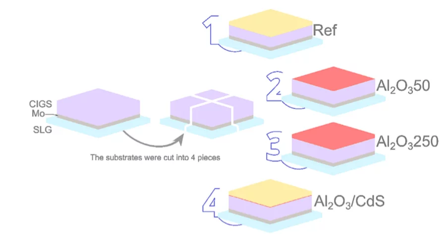
In the past years, the strategies used to break the Cu(In,Ga)Se2 (CIGS) light to power conversion effi- ciency world record value were based on improvements of the absorber optoelectronic and crystalline properties, mainly using complex post-deposition treatments. To reach even higher efficiency values, fur- ther advances in the solar cell architecture are needed, in particular, with respect to the CIGS interfaces. In this study, we evaluate the structural, morphological and optoelectronic impact of an Al2O3 layer as a potential front passivation layer on the CIGS properties, as well as an Al2O3 tunneling layer between CIGS and CdS. Morphological and structural analyses reveal that the use of Al2O3 alone is not detrimental to CIGS, although it does not resist to the CdS chemical bath deposition. The CIGS optoelectronic properties degrade when the CdS is deposited on top of Al2O3. Nonetheless, when Al2O3 is used alone, the opto- electronic measurements reveal a positive impact of this inclusion such as a very low concentration of interface defects while keeping the same CIGS recombination channels. Thus, we suggest that an Al2O3 front passivation layer can be successfully used with alternative buffer layers. Depth-resolved microscopic analysis of the CIGS interface with slow-muons strongly suggests for the first time that low-energy muon spin spectroscopy (LE-μSR) is sensitive to both charge carrier separation and bulk recombination in com- plex semiconductors. The demonstration that Al2O3 has the potential to be used as a front passivation layer is of significant importance, considering that Al2O3 has been widely studied as rear interface passi- vation material.
Facility: SμS
Reference: M.A. Curado et al, Applied Material Today 21, 100867 (2020)
Read full article: here


