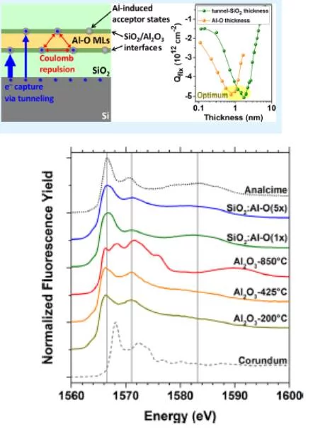
In high-efficiency silicon photovoltaics so-called carrier-selective passivating contacts are currently in the focus of research. Such materials allow for both very little charge carrier recombination at the interface between the silicon and the contact material, and low contact resistivities. In other words, an ideal carrier-selective passivating contact allows for the unobstructed transition of one type of charge carrier (electrons or holes), while preventing the other one to reach the contact. Dielectrics such as SiO2, SiNx, or Al2O3 provide very low defect densities at the Si/dielectric interface and thereby a good surface passivation. In some cases, the presence of fixed charges in the dielectric allows for additional field-effect passivation, i.e., charge carriers with the same polarity as the fixed charge are repelled from the surface, which prevents recombination at surface defects. However, dielectric thin films with thicknesses beyond 10 nm are highly insulating, so that they cannot serve as a contact material. On the other hand, materials with a good conductivity such as metals or transparent conductive oxides usually imply very high recombination losses. Materials that provide a trade-off between both parameters must be found, such as ultra-thin films of dielectrics that passivate the surface and allow for direct quantum mechanical tunneling. In this fundamental study, we investigated the structural properties of Al-O monolayers deposited by atomic layer deposition (ALD) in ultra-thin SiO2 layers with a variety of methods. Using synchrotron X-ray absorption spectroscopy (XANES) at the Al K-edge (PHOENIX beamline, SLS), we investigated the bonding configuration and local atomic surrounding of Al-atoms in Al-O monolayers embedded in SiO2 in comparison to conventional ALD-Al2O3 thin films. It turns out that Al-atoms in the Al-O monolayers are solely tetrahedrally coordinated (AlO4) and cannot undergo a phase transition (crystallization) at high temperatures, in contrast to the Al2O3 thin films. In the extended X-ray absorption fine structure (EXAFS) we observed that the Al–O bond length in the monolayers is shorter than in Al2O3 and approaches the length of the adjacent Si–O bonds, in agreement with density functional theory (DFT) calculations. Based on these structural investigations a new model was developed to explain the origin of the negative fixed charge at the SiO2/Al-O interface and the passivation of Si/SiO2 interface defects.
Contact
Dr. Daniel HillerResearch School of Engineering
Australian National University (ANU), Canberra, Australia
E-mail: daniel.hiller@anu.edu.au
Dr. Jörg Göttlicher
Institute for Photon Science and Synchrotron Radiation
Karlsruhe Institute of Technology, Germany
E-Mail: joerg.goettlicher@iss.fzk.de
Dr. Thomas Huthwelker
Swiss Light Source
Paul Scherrer Institut
Telephone: +41 56 310 5314
E-mail: thomas.huthwelker@psi.ch
Original Publication
Structural Properties of Al−O Monolayers in SiO2 on Silicon and the Maximization of Their Negative Fixed Charge DensityDaniel Hiller, Jörg Göttlicher, Ralph Steininger, Thomas Huthwelker, Jaakko Julin, Frans Munnik, Michael Wahl, Wolfgang Bock, Ben Schoenaers, Andre Stesmans, Dirk König
ACS Applied Materials & Interfaces 2018, 10, 30495−30505, 15 Aug 2018
DOI: https://doi.org/10.1021/acsami.8b06098
