Thin films are a very important field of research and application. Often, the surface of thin films determines many properties such as beauty. But beauty is only skin deep, and it is only the skin you see (15th century proverb). Therefore thin films presents often the amount of material necessary to accomplish something. Thin-film technology is one of the oldest arts and at the same time one of the newest sciences dating back to the metal ages of antiquity.
Deposition Techniques
The deposition techniques are usually divided into physical (e.g. PLD) and chemical (e.g. CVD) methods. Thin films are prepared from inorganic, organic or even biological materials and are nowadays applied as protective coatings, decoration, as structural and electronic materials and in optics (e.g. mirrors), etc., while the most important polymeric materials are photoresists (deposited by spincoating). Recently, the deposition of sensitive organic/polymeric (multi-)layers and biological samples became also an important research topic. Laser ablation is also used to create nano-particles in liquid by ablating from a metal target. Examples of metal ablation in liquid (and others) are shown on the web pages of Prof. Barcikowski's Group at the University of Duisburg.
Pulsed Laser Deposition (PLD)
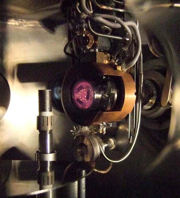
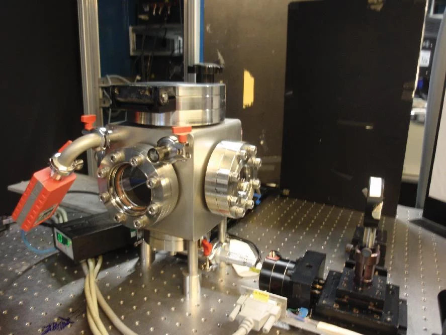
Pulsed Laser deposition is a very suitable technique compared to other deposition methods for the controlled deposition of complex multielemental thin films with a desired stoichiometry. For PLD a high power laser is used as an external energy source that interacts with a target and vaporizes this material. The evaporated material forms a plasma plume and is deposited on a heated substrate. The deposited material can range from nano-particles to thin films (amorphous - polycrystalline - single crystalline) that can contain stress, which may vary the film properties. How such an ablation process looks like is shown in the following image and video in one of our PLD chambers. Here, the ionic conductor YSZ is ablated using a 193nm excimer laser onto a heater. Normally, the sintered ceramic (cylindrical target) shows a white colour. Due to the intens interaction with the UV laser light, oxygen is removed and YSZ turns black. This is called incubation and common for quite a number of other ceramics such as SrTiO3 or MgO during ablation.
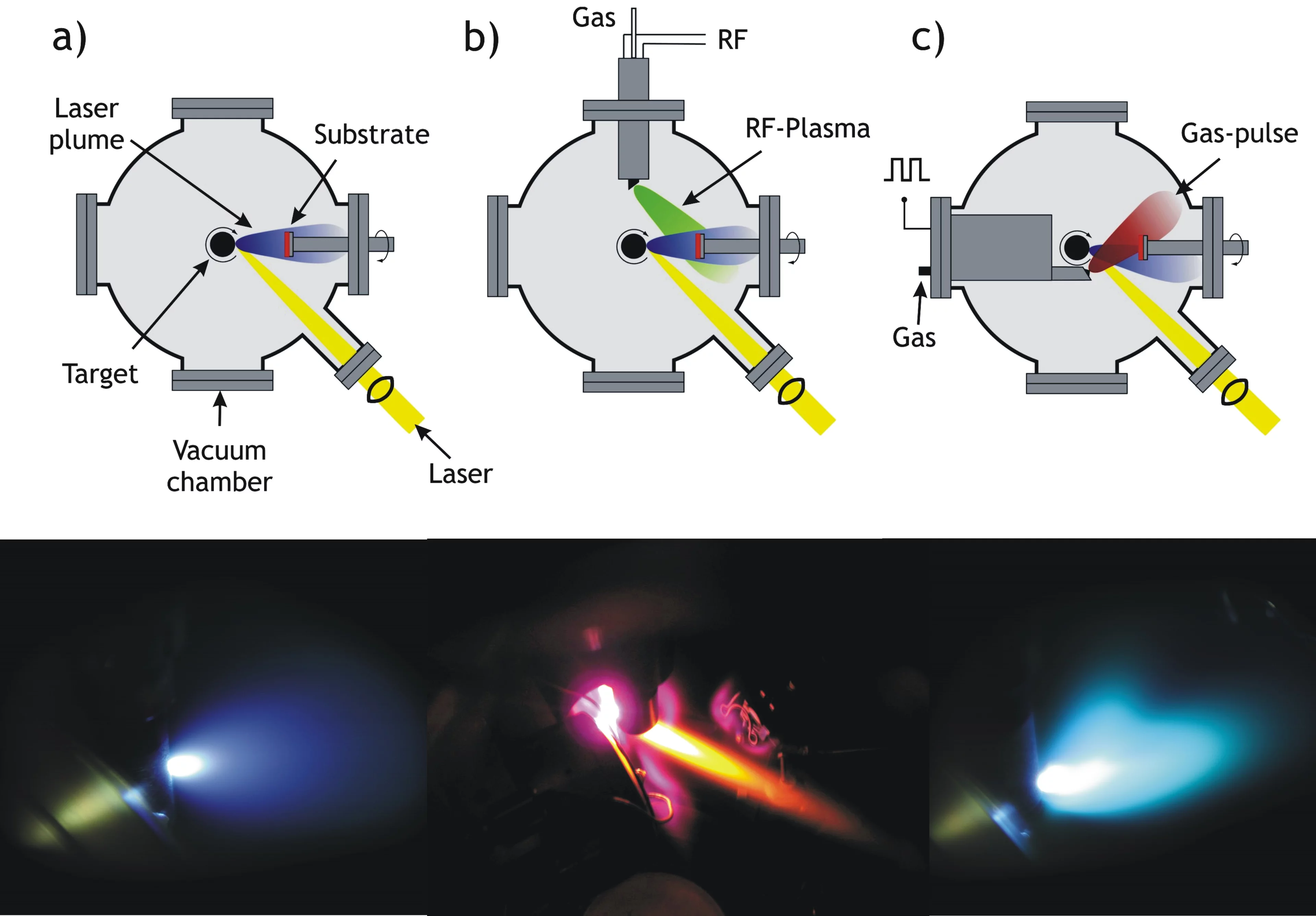
There are at least three different realizations of PLD in use today. Most common is the "classical" PLD set-up (a). The other two variations, RF Plasma assisted PLD (b) and Pulsed Reactive Crossed-Beam Laser Ablation (PRCLA) (c), provide more options to do in situ plasma chemistry. All three techniques are shown schematically and with an image next.
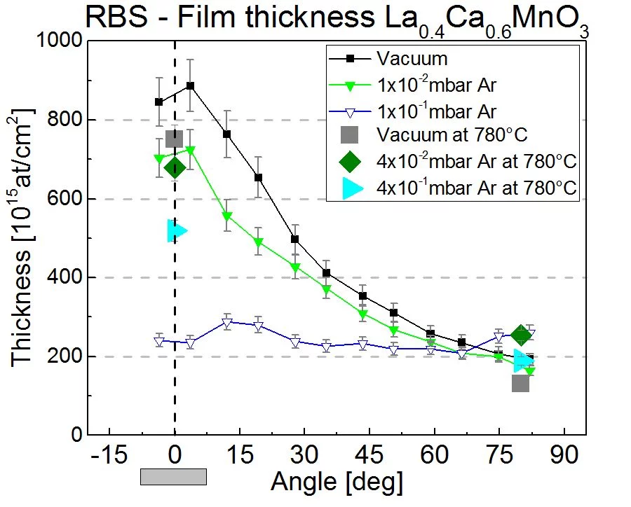
The pressure to deposit thin films by PLD ranges from vacuum to almost 1 mbar. This is much larger than any other PVD or CVD deposition technique and provids a lot of flexibility for the deposition process. The main purpose to add a background gas is to control the kinetic energy of the plasma species. At a low pressure (<10-2mbar), where the mean free path is much longer than the typical substrate-target distance, the kinetic energy can be as large as several 100eV. At 0.1mbar, the kinetic energies of plasma speces is slowed down to a few and up to some 10eV as a result of the formation of a shock-wave at the front of the expanding plasma plume. The expantion of the plasma species is very directional, in particular at a lower pressure and has a pronounced angular dependence. This is shown in the next image where the thickness and composition of ablated La0.6Ca0.6MnO3 has been measured vs. deposition angle using Rutherford back scattering at the ion beam physics group, ETH Zurich. The deposition was done in vacuum, 1x10⁻² and 1x10⁻¹ Ar background pressure. More details can be found here.
The most common background gas added for oxide ablation is O2 to improve the oxygen content in a film. With increasing pressure, the number of scattering events during the expansion of the plasma increases. Therefore the intensity of the visible light from the expanding plume increases due to an increase of re-excitations in the plamsa. This increase in luminosity due to an increase in scattering events is an indirect measure of an increase in chemical activity in the plasma. This is shown in the next image. Other background gases used for ablation are N2O or NO2 to provede a more reactive atmosphere. To prepare nitrides or oxinitrids, N2 or NH3 have also been used.
RF Plasma assisted PLD
In RF plasma beam assisted PLD, a plasma beam is directed toward the substrate surface in order to supply reactive species, such as atomic/diatomic excited oxygen during film growth. This can be utilized to introduce and control the amount of light elements in thin films.
Pulsed Reactive Crossed-Beam Laser Ablation
In Pulsed Reactive Crossed-Beam Laser Ablation (PRCLA) a synchronized gas pulse crosses the ablation plume close to its origin, increasing the gas phase interaction (see larger plasma plume in the picture) and the probability of reactive scattering. This allows the resulting species to propagate freely away from the localized scattering region. PRCLA is especially suited for the deposition of oxides, nitrides and carbides where the gas pulse is utilized to introduce the light elements into the films. The gas pulse pressure and background pressure even allow to control the oxygen content in certain perovskite films.
Metal-Organic Chemical Vapor Deposition (MOCVD)
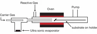
Metal-Organic Chemical Vapor Deposition (MOCVD) belongs to the class of chemical thin film deposition methods and is quite similar to other techniques, such as spray pyrolysis, where the vaporization method and the precursors may vary. It is in principle a simple "non-vacuum" technique, which allows the fast deposition of various film materials without using a laser. The films are normally polycrystalline and can be quite smooth.
Laser-Induced Forward Transfer (LIFT)
(in collaboration with the Laboratory for Functional Polymers at EMPA)
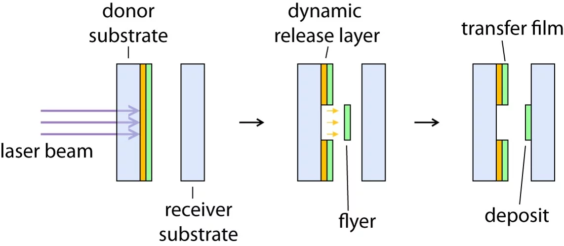
LIFT belongs to the class of deposition methods, which utilize lasers to transfer a thin material layer with a resolution in the micron range from a target to a receiver material. The quality of the thin layers may be superior to other deposition techniques. Many different modification of this approach exist which vary in the utilized laser, additional materials, or the conditions, e.g. vacuum. Examples of these techniques are:
- LAT = laser ablation transfer
- LITI = laser-induced thermal imaging
- MAPLE = matrix-assisted pulsed laser evaporation
- MAPLE DW = matrix-assisted pulsed laser evaporation-direct write
- LMI = Laser molecular implantation
All these methods have the advantage that they are "solvent" free deposition techniques, which allow to deposit multilayers without the need to identify suitable solvent systems or to obtain a polymer that can be evaporated thermally. With the exception of MAPLE, all other LIFT approaches allow a deposition with a "high" lateral resolution. More information to LIFT and respective applications can be found here.
Spin Coating
Spin coating is a cheap and fast method to produce homogeneous layers. An excess amount of the solvent is placed on the substrate, which is then rotated at high speed in order to spread the fluid by centrifugal force. The film thickness can be adjusted by varying the rotation speed, the rotation time, and the concentration of the used solution. The disadvantage of this method is that it is limited by the solvent and that no lateral resolution is possible.
Epitaxy and Strain in Thin Films
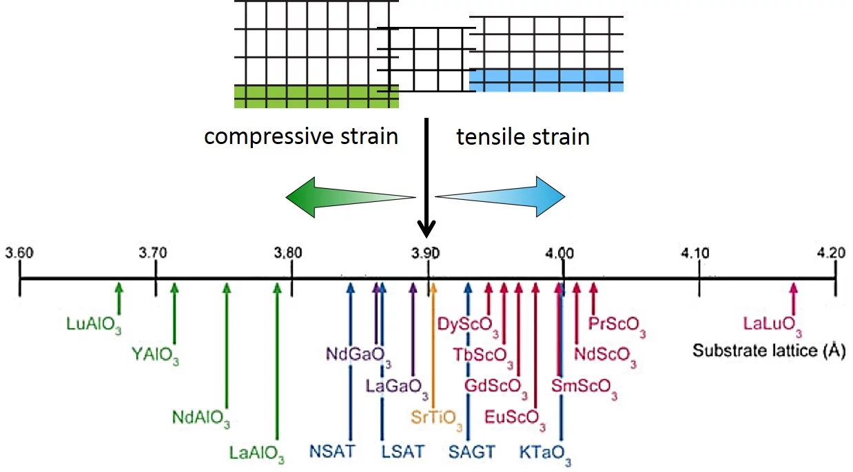
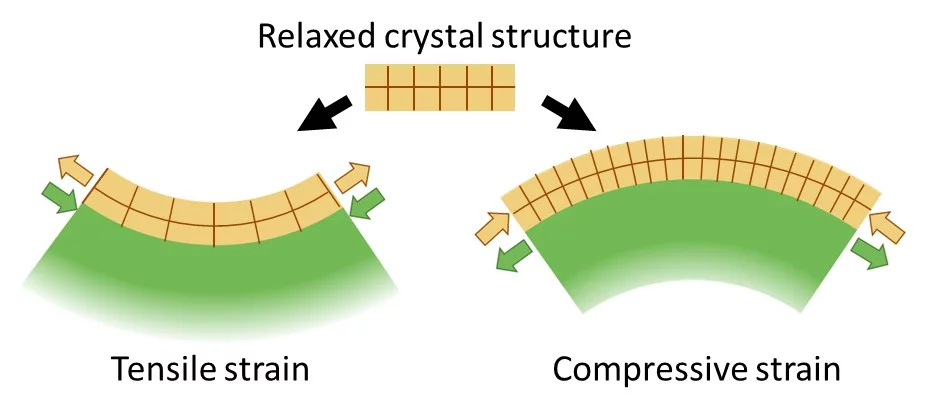
To improve, modify or change material properties, there are a number of ways to accomplish this. The most common route is chemical substitution. Without changing the composition, physical properties can be significantly altered by changing the microstructure like grain size or porosity. Likewise physical properties can be changed through lattice distortions (strain). Applying strain to a crystal changes the bond lengths and subsequently the electron density or the orbital overlap. As a result, physicochemical characteristics can be strongly influenced. Material properties may be enhanced or inhibited or new functionalities emerge. Strain affects materials in many different ways like the electronic bandgap, the behaviour of correlated systems, thermal conductivity, multiferroicity, catalytic properties or charge transport. The tuning of material properties via lattice distortions is referred to as strain engineering.
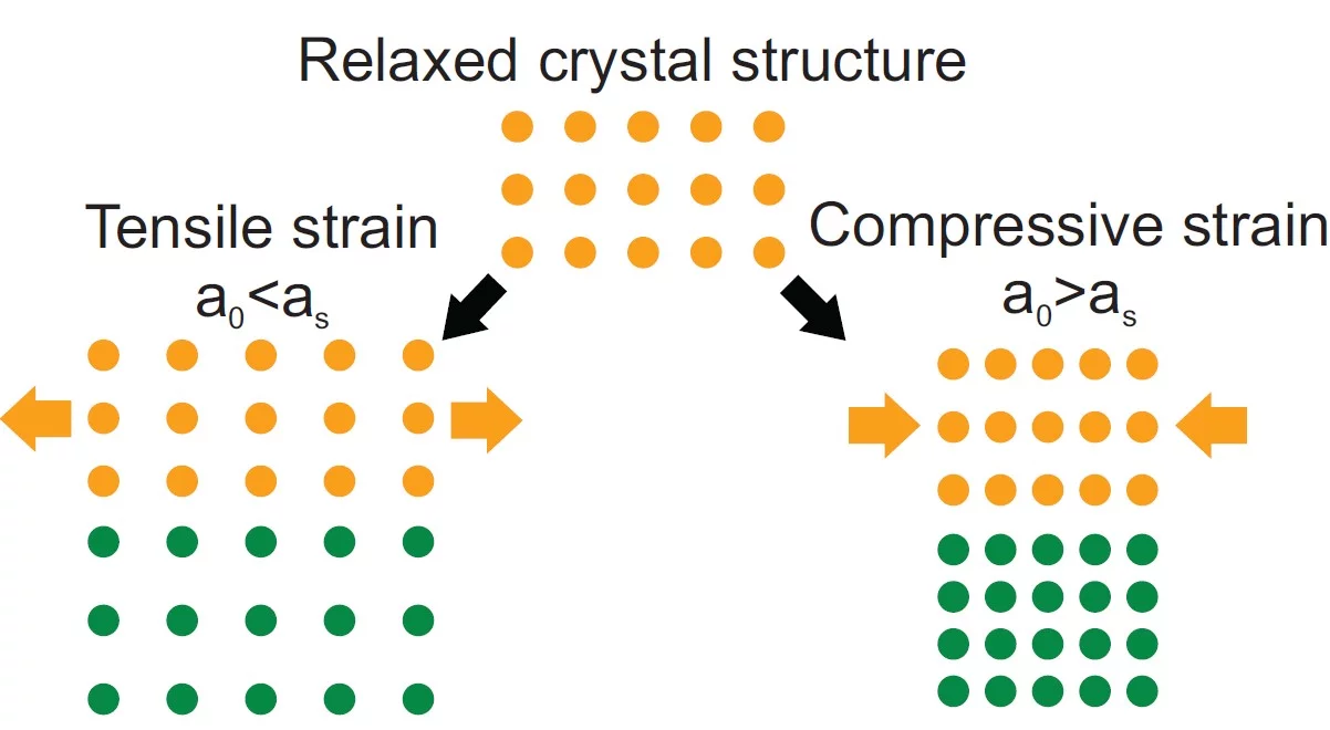
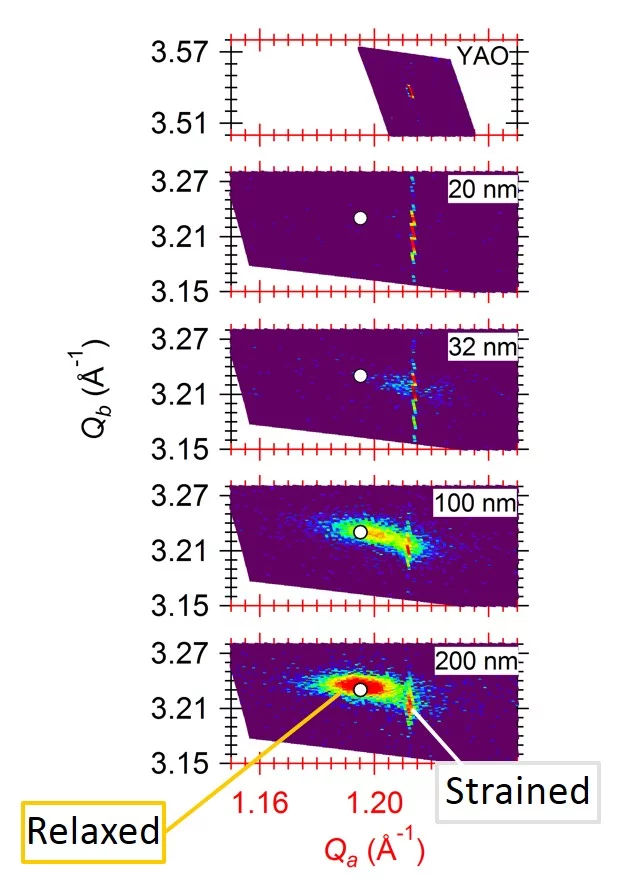
Strain in an epitaxial film develops due to the mismatch of the lattice constants between film (a0) and substrate (as) and is expressed as f = (as - a0)/a0. When a film grows epitaxially on a substrate, the material tries to be smoothly connected to the substrate and to avoid forming dangling bonds. As a consequence, the film initially tends to grow with its in-plane lattice parameters fixed to those of the substrate. In a thin film the strain/stress is simultaneously applied along two in-plane directions (biaxial strain) while the third (out-of-plane) is free to adapt. Perfect coupling between the film and substrate in-plane lattice is called pseudomorphic growth and the interface is coherent. In the case of a pseudomorphic growth, a = as and f = ε. Due to imperfections in the crystal lattice, the interface, or due to the surface morphology of the film, the in-plane lattice constant of the film can also only partially adapt to the substrate, or even be fully relaxed (|ε| < |f|). The strain will relax as a function of the film thickness through the introduction of crystalline defects that reduces the elastic energy in the film. A lattice mismatch |f| ≤ 1% is considered to be "small" and may be expected to be fully accommodated. In perovskites, larger mismatch values can be accommodated by deviations e.g. by tilting of the oxygen octahedra. The largest lattice mismatch value reported so far to be accommodated by strain is 6.6 % for BiFeO3 grown on (110) YAlO3 (R.J. Zeches et al., Science 326 , 977 (2009)).
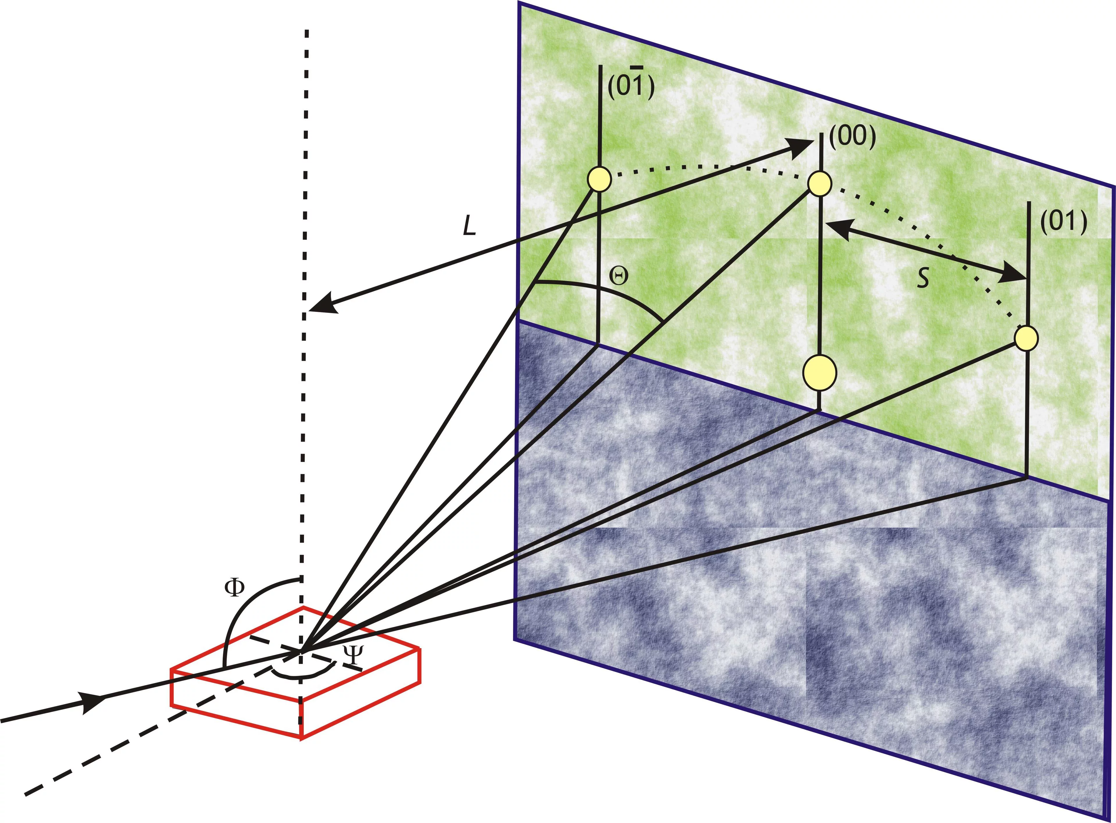
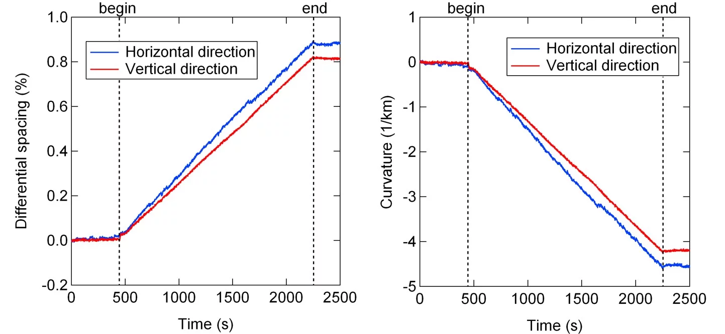
The figure shows a MOSS measurement during the deposition of 3YSZ on (001) silicon at room temperature along the horizontal and vertical direction. With increasing thickness (time) the differential spacing of the spots on the surface changes linearely, which corresponds to a linear change in curvature with increasing thickness. Graphs by Dieter Stender.

