

LHC/CMS Particle Tracking Upgrade (PSI46dig)
(Project in collaboration with the LTP HEP Group)
"PSI46" is the identification of the Readout Chips used in the innermost particle tracking system of the CERN/LHC/CMS pixel detector unit. The challenges posed by the much higher luminosity forecasted for the LHC after its first upgrade makes "PSI46" not suited to stand the increased flux of the particles to track. To target this problem a revised version of the chip was designed (PSI46dig), where several improvements have been implemented:
| PSI46 | PSI46dig | PROC600 | |
|---|---|---|---|
| Technology | 0.25μm IBM | 0.25μm IBM | 0.25μm IBM |
| Chip size | 7.9 x 10.0 mm2 | 7.9 x 10.3 mm2 | 7.9 x 10.6 mm2 |
| Pixel size | 150 x 100μm2 | 150 x 100μm2 | 150 x 100μm2 |
| Pixel array | 52 x 80 | 52 x 80 | 52 x 80 |
| Transistor count | 1.3 Mio | 1.4 Mio | 2.2 Mio |
| Readout | multi level @ 40 MHz | 160 MBit/sec | 160 MBit/sec |
| Hit rate | 80 MHz/cm2 | 120 MHz/cm2 | 600 MHz/cm2 |
| Radiation tolerance | 200 kGy | 1 MGy | 6 MGy |
EIGER hybrid photon counting chips for X-rays
The EIGER chip is a hybrid photon counting, mixed-mode pixel chip for X-ray radiation detection with radiation-tolerant design and high framing rate. The chip, designed in CMOS 0.25μm technology, is an array of 256 x 256 “active” pixels, each 75x75μm2. Each pixel contains a preamplifier, shaper, discriminator and a configurable 12 bit counter; plus temporary storage, readout, control and test circuitry. During the “Expose” phase, every incoming photon which exceeds a pre-selectable energy threshold increments the counter by 1 count. During the “Readout” phase the values stored in the counters are readout via a 32 line parallel bus. The chip can perform simultaneous expose-readout, and can reach a frame rate of about 12 kHz, when the counter is set in 8-bit mode (default). The low dead time between frames (~2μs) and the continuous readout make the depth of the on-pixel counter not limiting the achievable dynamic range. From a radiation tolerance point of view, the chip should in principle be able to work up to several Mrads without any action by the user, and at even higher radiation levels with minor modifications of the bias voltages.
The chip will be used as a radiation-tolerant, high frame rate X-ray imager in Synchrotron beamlines. The main targeted applications are: Protein Crystallography, Coherent Small Angle X-ray Scattering, Scanning Small Angle X-ray Scattering, Coherent Diffractive Imaging, X-ray Photon Correlation Spectroscopy. The chip specifications are shortly reported here:
| EIGER specifications | |
|---|---|
| Technological process | UMC 0.25μm |
| Radiation tolerance | Full tolerant design (>4Mrad) |
| Chip size | 2 x 2 cm2 |
| Pixel size | 75 x 75μm2 |
| Pixel array | 256 x 256, i.e. 65'536 pixel |
| Count rate | 3.4 x 10⁹ X-rays/mm2/sec |
| " | i.e. 1..2 Mcounts/pixel/sec |
| Counter | 12 bits, binary, double buffered, |
| " | configurable (4,8,12 bit mode) |
| Continuous readout | yes |
| Detector readout speed | 12 kHz @ 8 bit & 23 kHz @ 4 bit mode, |
| " | Detector size doesn't matter |
| Transistor count | 30 Million |
| Noise | 100 e- rms (in medium gain mode) |
| Threshold dispersion | 25 e- rms (in medium gain mode) |
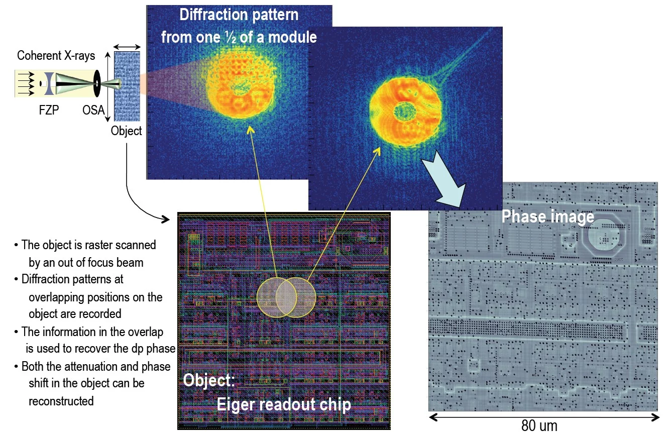
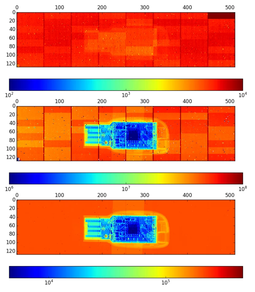
An EIGER selfie by using ptychography:
A very peculiar application of EIGER is ptychography, where an object can be imaged with tens of nanometer resolution using a detector with pixel sizes in the order of tens of microns.
AGIPD hybrid photon integrating chips for X-rays
(Project in collaboration PSI-SLS detector group, DESY and University Hamburg, Bonn University)
The AGIPD is a high-speed detector intended for use at the European XFEL. It embeds in every pixel: preamplification with charge integration and dynamic gain switching, correlating double sampling, 352 analog storage cells, 704 digital storage cells plus readout circuitry. This peculiar design allows single-pulse imaging at 4.5 MHz frame rate for 352 frames and reliable detection of both single 12.4 keV photons and very intense signals of over 10,000 photons per pixel.
| AGIPD 1.0 chip specifications | |
|---|---|
| Technological process | IBM 130 nm |
| Chip size | 1.3 x 1.4 cm2 |
| Pixel size | 200 x 200μm2 |
| Pixel array | 64 x 64, i.e. 4'096 pixel |
| per pixel | - sensitive analog block layout: designed for radiation tolerance |
| " | - high speed preamp with dynamic gain switching and correlated double sampling |
| " | - 352 memory cells are optimized for radiation tolerance, too |
| chip | fast output buffers: > 40 Mhz sampling rate driving 100 Ohm loads |
| Noise | 265 e- rms |
MOENCH hybrid photon integrating chips for X-rays
(Project in collaboration PSI-SLS detector group and ETH Zurich)
MOENCH is a novel hybrid silicon pixel detector where charge integration (CI) is combined with a challengingly small pixel size of 25×25 μm2. CI enables the detector to process several incoming photons simultaneously in XFEL applications. Moreover, due to the small pixel size, the charge produced by an impinging photon is often shared. In low flux experiments the analog information provided by single photons can be used either to obtain spectral information or to improve the position resolution by interpolation. Possible applications are resonant and non-resonant inelastic X-ray scattering or X-ray tomography with X-ray tubes.
| MOENCH 03 chip specifications | |
|---|---|
| Technological process | UMC 110 nm |
| Active area | 10 x 10 cm2 |
| Chip size | 1.2 x 1.2 cm2 |
| Pixel size | 25 x 25μm2 |
| Pixel array | 400 x 400, i.e. 160'000 pixel |
| " | - double side readout: 1 kHz, (6 kHz by design) |
| outputs | 32 differential lines (5 k pixels each) |
| Noise | 30 e- rms |

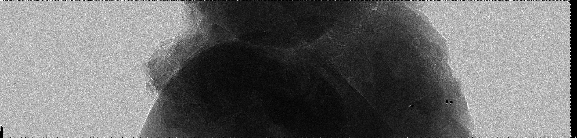
To test the imaging capability of MOENCH in interpolation mode, we took the image of a kidney stone at the Tomcat beamline at PSI (12 keV monochromatic beam); the test outcome is presented here:
DRS4 chip: allows for affordable "high speed oscilloscopes"
(Project in collaboration with the LTP Muon-Physics group)
The Domino Ring Sampler (DRS) is a family of Switched Capacitor Atrrays (SCA) chips developed to meet the high demands of modern experiments in fast waveform digitizing. The most recent version, DRS4, is produced in a radiation hard 0.25 um CMOS process, and is capable of digitizing 9 differential input channels at sampling rates of up to 6 Giga-samples per second (GSPS) with an analogue bandwidth of 950MHz(-3 dB). The channel depth can be configured between 1024 and 8192 cells, and the signal-to-noise ratio allows for solution equivalents to more than 11 bits. Using an interleaved sampling technique, sampling rates up to 48 GSPS are possible. Compared with the previous versions, the DRS4 chip contains several improvements such as an on-chip PLL for sampling-frequency stabilization and various mechanisms to reduce the readout dead-time. The high bandwidth, low power consumption and short readout time make this chip attractive for many experiments, replacing traditional ADC sand TDCs. This includes time-of-flight detectors, cosmic gamma ray observatories, PET scanners and industrial applications.
Performance comparison between a lab scope and a system based on the DRS4 chip:
| lab scope | DRS4 based | |
|---|---|---|
| channels | 4 | 8 (4 used) |
| sampling rate | 5 GSPS | 5 GSPS |
| analog BW | 1 GHz | ca. 1 GHz |
| resolution | 8 bit (6..7) | 11.5 |
| cost | 15 kEuro | 900 Euro |
| power | line | via USB |
Other Projects
The CDCT has also contributed to the development some other ASICs in collaboration with the SLS detector group:
- GOTTHARD: strip readout chip for X-ray detection at synchrotrons and XFELs based on charge integration
- JUNGFRAU: hybrid pixel chip for X-ray detection at XFELs and synchrotrons based on charge integration.
Some projects, again in collaboration with the SLS detector group, which are in a very early development phase, are:
- GOTTHARD II: strip readout chip for X-ray detection at XFELs and synchrotrons based on charge integration, with the ability to take >3k frames at ~200ns frame spacing.
- EIGER II: hybrid pixel chip for X-ray detection at synchrotrons based on single photon counting (Improved version of EIGER, to be designed in UMC110nm)
- MYTHEN III: strip readout chip for X-ray detection at synchrotrons based on single photon counting (Improved version of MYTHEN, to be designed in UMC110nm)
- UMC110nm RADIATION TOLERANCE campaign: The CDCT is carrying out a campaign to assess the radiation tolerance of the UMC110nm technology. This project is in collaboration with the the SLS detector group, the LTP-CMS group, the Universities of Padova and Bergamo (Italy) and DECTRIS.