Coexisting multiple order parameters in single-layer LuMnO3 films
Magnetoelectric multiferroics hold great promise for electrical control of magnetism or magnetic control of ferroelectricity. However, single phase ferroelectric materials with a sizeable ferromagnetic magnetization are rare. Here, we demonstrate that a single-phase orthorhombic LuMnO3 thin film features coexisting magnetic and ferroelectric orders.
In situ stress observation in oxide films and how tensile stress influences oxygen ion conduction
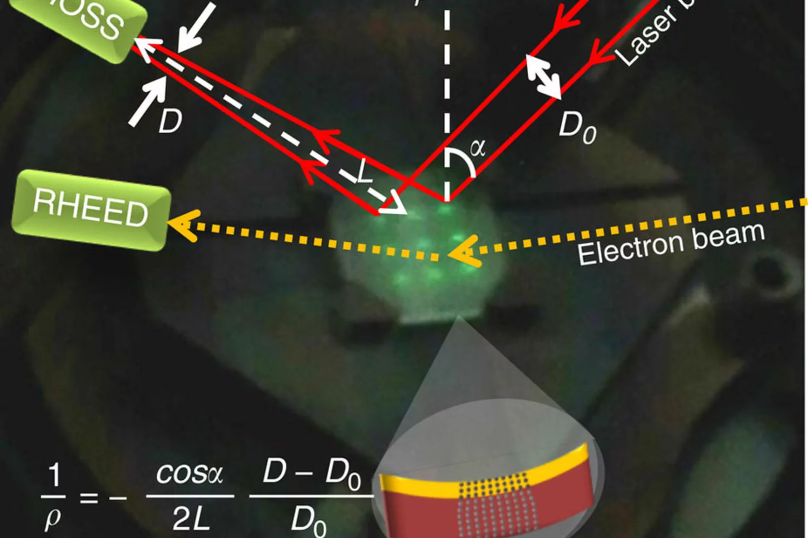
Many properties of materials can be changed by varying the interatomic distances in the crystal lattice by applying stress. Ideal model systems for investigations are heteroepitaxial thin films where lattice distortions can be induced by the crystallographic mismatch with the substrate. Here we describe an in situ simultaneous diagnostic of growth mode and stress during pulsed laser deposition of oxide thin films.
The flip-over effect in pulsed laser deposition: Is it relevant at high background gas pressures?
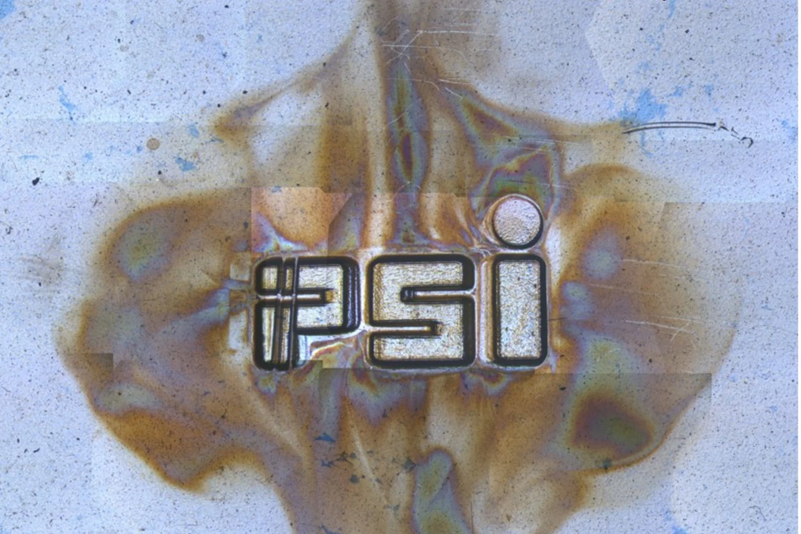
In pulsed laser deposition the use of a rectangular or elliptical beam spot with a non 1:1 aspect ratio leads to the so called flip-over effect. Here, the longest dimension of the laser spot results in the shortest direction of plasma plume expansion.
Interplay between magnetic order at Mn and Tm sites alongside the structural distortion in multiferroic films of o-TmMnO3
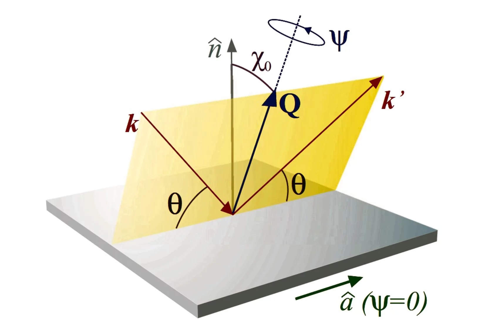
We employ resonant soft x-ray diffraction to individually study the magnetic ordering of the Mn and the Tm sublattices in single-crystalline films of orthorhombic (o−)TmMnO3. The same magnetic ordering wave vector of (0q0) with q≈0.46 is found for both ionic species, suggesting that the familiar antiferromagnetic order of the Mn ions induces a magnetic order on the Tm unpaired 4f electrons.
Crystallization of zirconia based thin films
In pulsed laser deposition the use of a rectangular or elliptical beam spot with a non 1:1 aspect ratio leads to the so called flip-over effect. Here, the longest dimension of the laser spot results in the shortest direction of plasma plume expansion.
Multiferroic Properties of o−LuMnO3 Controlled by b-Axis Strain
Strain is a leading candidate for controlling magnetoelectric coupling in multiferroics. Here, we use x-ray diffraction to study the coupling between magnetic order and structural distortion in epitaxial films of the orthorhombic (o-) perovskite LuMnO3. An antiferromagnetic spin canting in the E-type magnetic structure is shown to be related to the ferroelectrically induced structural distortion and to a change in the magnetic propagation vector.
Low-temperature solid-oxide fuel cells based on proton-conducting electrolytes
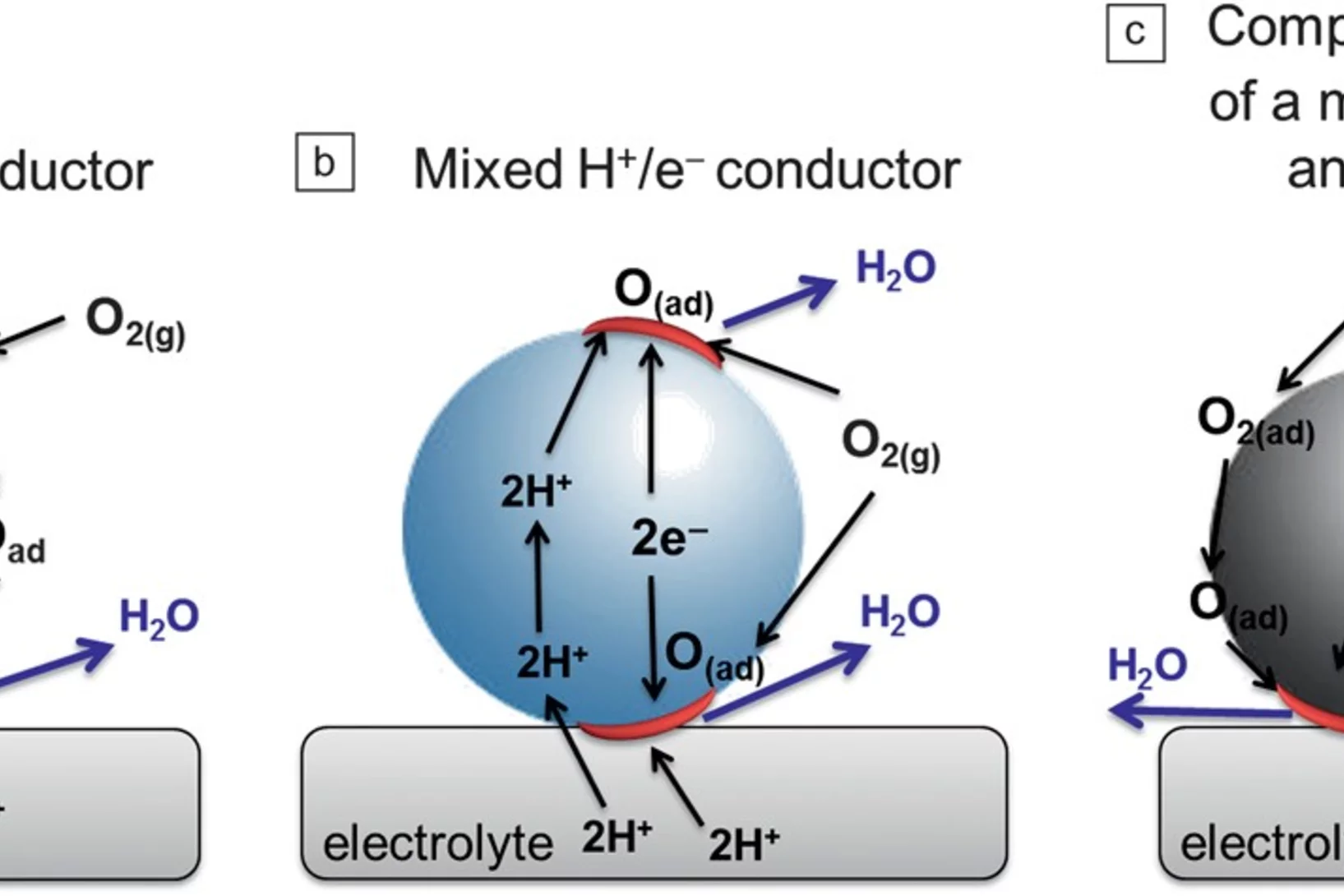
The need for reducing the operating temperature of solid-oxide fuel cells (SOFCs) imposed by cost reduction has pushed significant progress in fundamental understanding of the individual components, as well as materials innovation and device engineering. Proton-conducting oxides have emerged as potential alternative electrolyte materials to oxygen-ion conducting oxides for operation at low and intermediate temperatures.
Plasma interactions determine the composition in pulsed laser deposited thin films
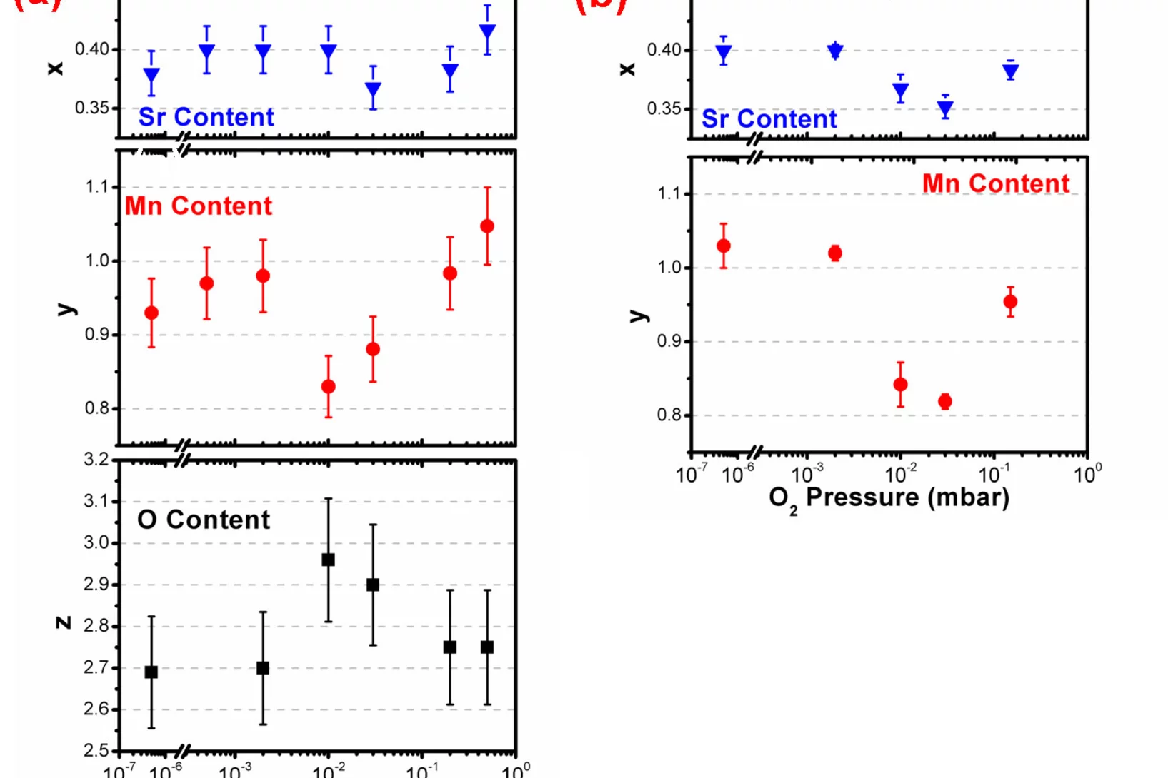
Plasma chemistry and scattering strongly affect the congruent, elemental transfer during pulsed laser deposition of target metal species in an oxygen atmosphere. Studying the plasma properties of La0.6Sr0.4MnO3, we demonstrate for as grown La0.6Sr0.4MnO3-δ films that a congruent transfer of metallic species is achieved in two pressure windows: ∼10−3 mbar and ∼2 × 10⁻¹ mbar.
Determination of conduction and valence band electronic structure of La2Ti2O7 thin film
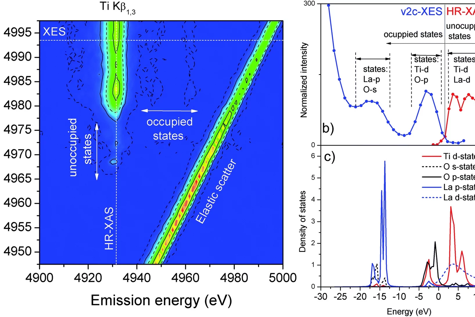
The electronic structure of a La2Ti2O7-layered perovskite thin film was determined by resonant inelastic X-ray scattering (RIXS) measurements and FEFF calculations. It was found that the empty Ti and La d-band states dominate the conduction band of the structure, whereas the top edge of the valence band is mainly composed of filled O-p states. Furthermore, there is a pronounced overlap between occupied La-p states and O-s states, which are located deeper in the valence band.
Magnetismus im Stress: Gleichzeitiger Anti- und Ferromagnetismus
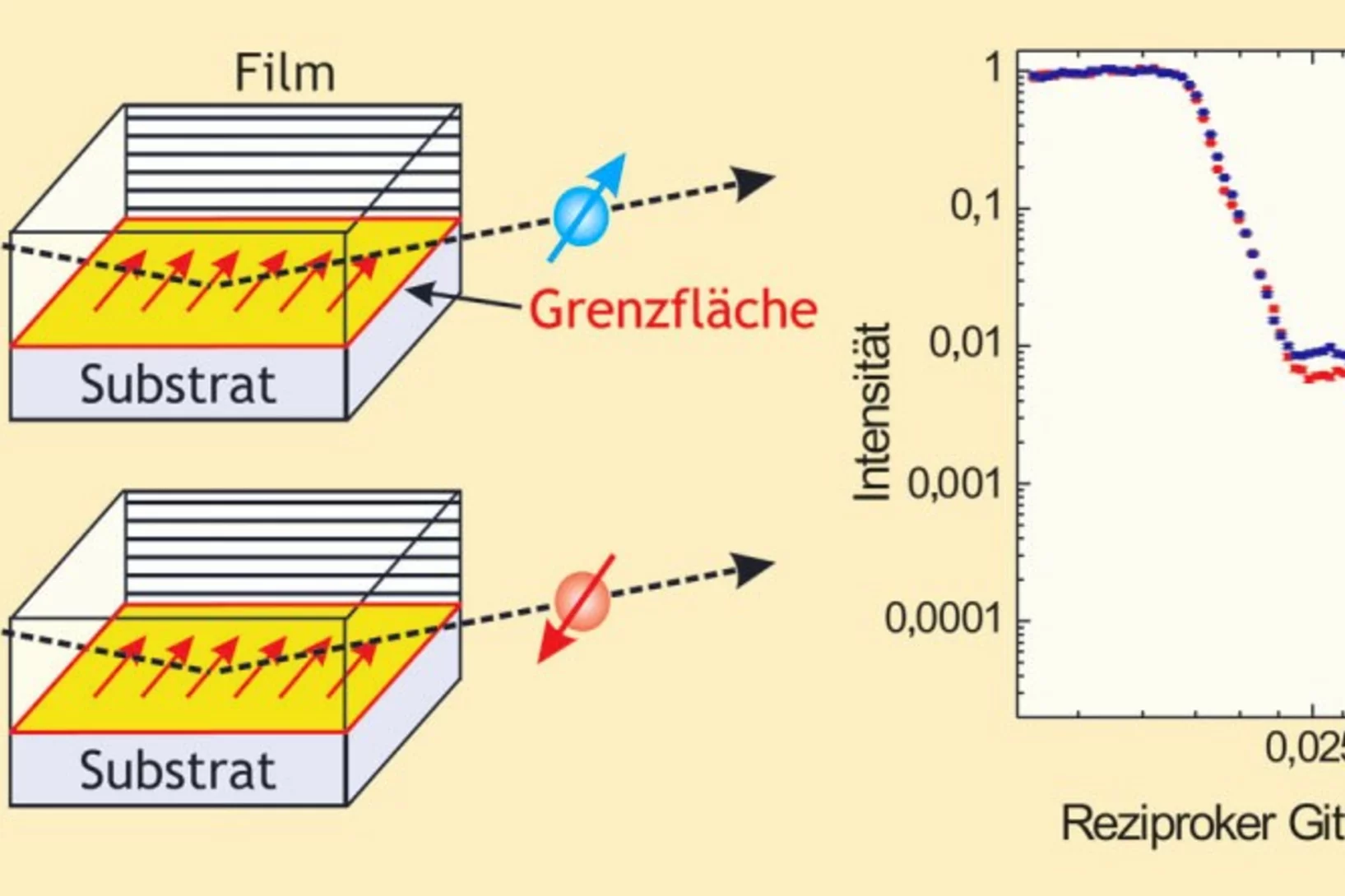
Die gleichzeitige Existenz von Magnetismus und Ferroelektrizät in einem Material ist selten. Setzt sich dieser Magnetismus aus mehreren unabhängigen, magnetischen Grundzuständen zusammen, ist das ungewöhnlich. Einer schweizerisch-französischen Zusammenarbeit unter Leitung des Paul Scherrer Instituts ist es gelungen, mehrere magnetische Grundzustände in einem Material zu realisieren und detailliert zu untersuchen.
Interface superconductor with gap behaviour like a high-temperature superconductor
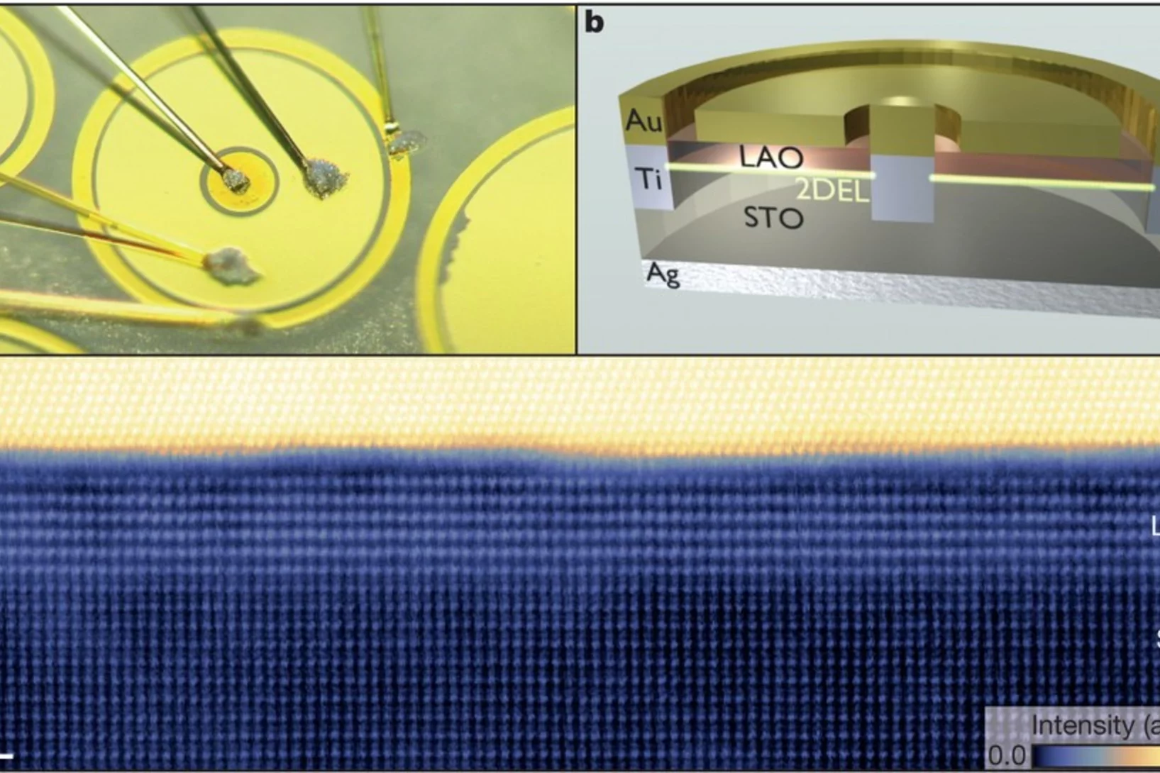
The physics of the superconducting state in two-dimensional (2D) electron systems is relevant to understanding the high-transition-temperature copper oxide superconductors and for the development of future superconductors based on interface electron systems. But it is not yet understood how fundamental superconducting parameters, such as the spectral density of states, change when these superconducting electron systems are depleted of charge carriers.
Strain-Induced Ferromagnetism in Antiferromagnetic LuMnO3 Thin Films
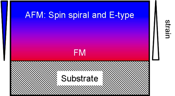
Single phase and strained LuMnO3 thin films are discovered to display coexisting ferromagnetic and antiferromagnetic orders. A large moment ferromagnetism (≈1μB), which is absent in bulk samples, is shown to display a magnetic moment distribution that is peaked at the highly strained substrate-film interface. We further show that the strain-induced ferromagnetism and the antiferromagnetic order are coupled via an exchange field, therefore demonstrating strained rare-earth manganite thin films as promising candidate systems for new multifunctional devices.
On Proton Conductivity in Porous and Dense Yttria Stabilized Zirconia at Low Temperature
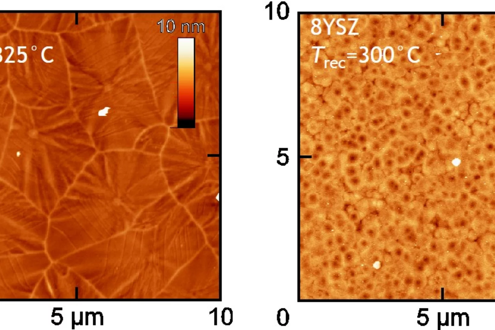
The electrical conductivity of dense and nanoporous zirconia-based thin films is compared to results obtained on bulk yttria stabilized zirconia (YSZ) ceramics. Different thin film preparation methods are used in order to vary grain size, grain shape, and porosity of the thin films. In porous films, a rather high conductivity is found at room temperature which decreases with increasing temperature to 120 °C. This conductivity is attributed to proton conduction along physisorbed water (Grotthuss mechanism) at the inner surfaces.
Applications of laser printing for organic electronics
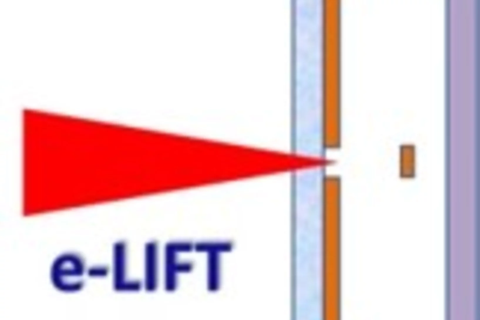
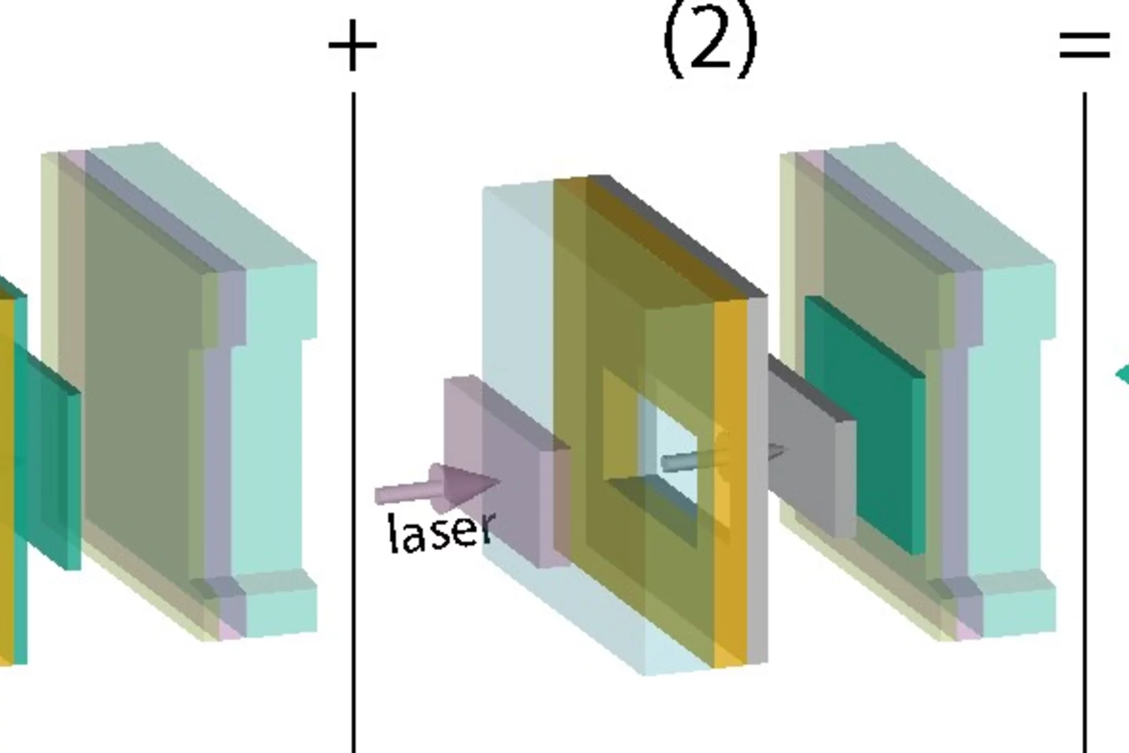
The development of organic electronic requires a non contact digital printing process. The European funded e-LIFT project investigated the possibility of using the Laser Induced Forward Transfer (LIFT) technique to address this field of applications. This process has been optimized for the deposition of functional organic and inorganic materials in liquid and solid phase, and a set of polymer dynamic release layer (DRL) has been developed to allow a safe transfer of a large range of thin films.
Electric-Field-Induced Polar Order and Localization of the Confined Electrons in LaAlO3/SrTiO3 Heterostructures
With ellipsometry, x-ray diffraction, and resistance measurements we investigated the electric-field effect on the confined electrons at the LaAlO3/SrTiO3 interface. We obtained evidence that the localization of the electrons at negative gate voltage is induced, or at least enhanced, by a polar phase transition in SrTiO3 which strongly reduces the lattice polarizability and the subsequent screening. In particular, we show that the charge localization and the polar order of SrTiO3 both develop below ∼50 K and exhibit similar, unipolar hysteresis loops as a function of the gate voltage.
The fabrication of small molecule organic light-emitting diode pixels by laser-induced forward transfer
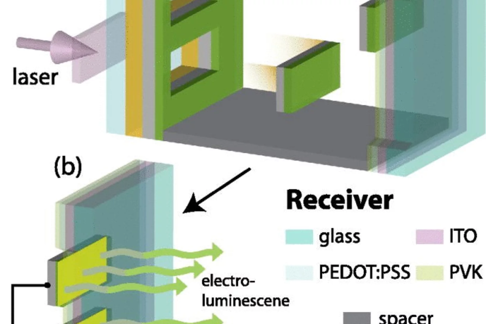
Laser-induced forward transfer (LIFT) is a versatile organic light-emitting diode (OLED) pixel deposition process, but has hitherto been applied exclusively to polymeric materials. Here, a modified LIFT process has been used to fabricate small molecule Alq3 organic light-emitting diodes (SMOLEDs). Small molecule thin films are considerably more mechanically brittle than polymeric thin films, which posed significant challenges for LIFT of these materials.
Laser-Induced Forward Transfer for the Fabrication of Devices
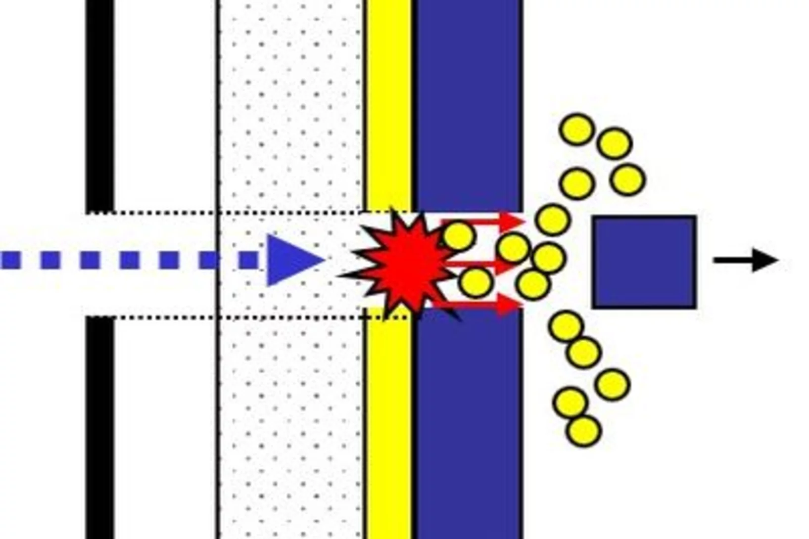
In conjunction with the increasing availability of cost-efficient laser units during the recent years, laser-based micromachining techniques have been developed as an indispensable industrial instrument of ‘‘tool-free’’ high-precision manufacturing techniques for the production of miniaturized devices made of nearly every type of materials. Laser cutting and drilling, as well as surface etching, have grown meanwhile to mature standard methods in laser micromachining applications where a well-defined laser beam is used to remove material by laser ablation. As an accurately triggerable nonmechanical tool, the ablating laser beam directly allows a subtractive direct-write engraving of precise microscopic structure patterns on surfaces, such as microchannels, grooves, and well arrays, as well as for security features. Therefore, laser direct-write (LDW) techniques imply originally a controlled material ablation to create a patterned surface with spatially resolved three-dimensional structures, and gained importance as an alternative to complementary photolithographic wet-etch processes. However, with more extended setups, LDW techniques can also be utilized to deposit laterally resolved micropatterns on surfaces, which allows, in a general sense, for the laser-assisted ‘‘printing’’ of materials.
Tunable conductivity threshold at polar oxide interfaces
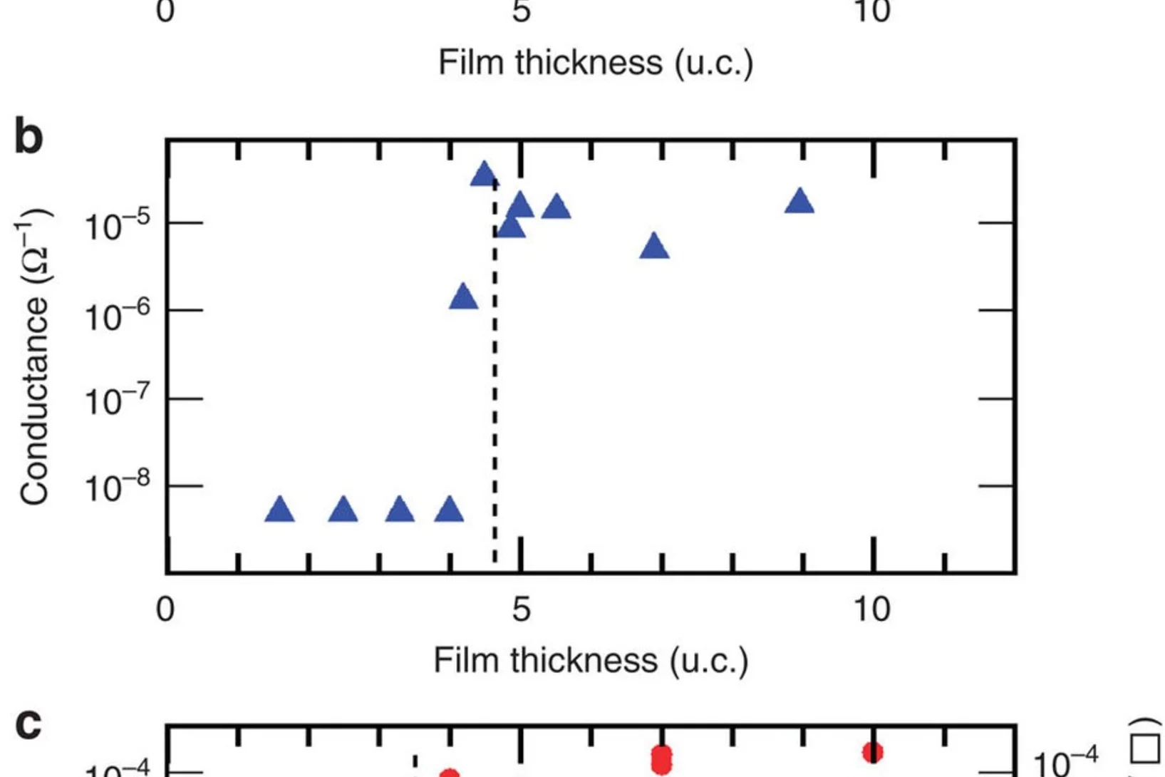
The physical mechanisms responsible for the formation of a two-dimensional electron gas at the interface between insulating SrTiO3 and LaAlO3 have remained a contentious subject since its discovery in 2004. Opinion is divided between an intrinsic mechanism involving the build-up of an internal electric potential due to the polar discontinuity at the interface between SrTiO3 and LaAlO3, and extrinsic mechanisms attributed to structural imperfections.
Sequential printing by laser-induced forward transfer to fabricate a polymer light-emitting diode pixel
Patterned deposition of polymer light-emitting diode (PLED) pixels is a challenge for electronic display applications. PLEDs have additional problems requiring solvent orthogonality of different materials in adjacent layers. We present the fabrication of a PLED pixel by the sequential deposition of two different layers with laser-induced forward transfer (LIFT), a “dry” deposition technique. This novel use of LIFT has been compared to “normal” LIFT, where all the layers are transferred in a single step, and a conventional PLED fabrication process.
Laser-Induced Forward Transfer for the Fabrication of Devices
X-ray near edge absorption spectroscopy was used to probe the electronic structure of multiferroic orthorhombic LuMnO3 polycrystalline samples and strained, twin-free orthorhombic (1–10) LuMnO3 films grown by pulsed laser deposition on (1–10) YAlO3 substrates. For all o-LuMnO3 samples x-ray near edge absorption spectroscopy spectra reveal that the pre-edge structure is influenced by the increase in MnO6 distortion as a result of the smaller Re-ion or film strain. Furthermore there is clear evidence of anisotropic Mn-O bonding and Mn orbital ordering along the c- and [110] direction. The experimental film and bulk data are in agreement with ab initio simulations.
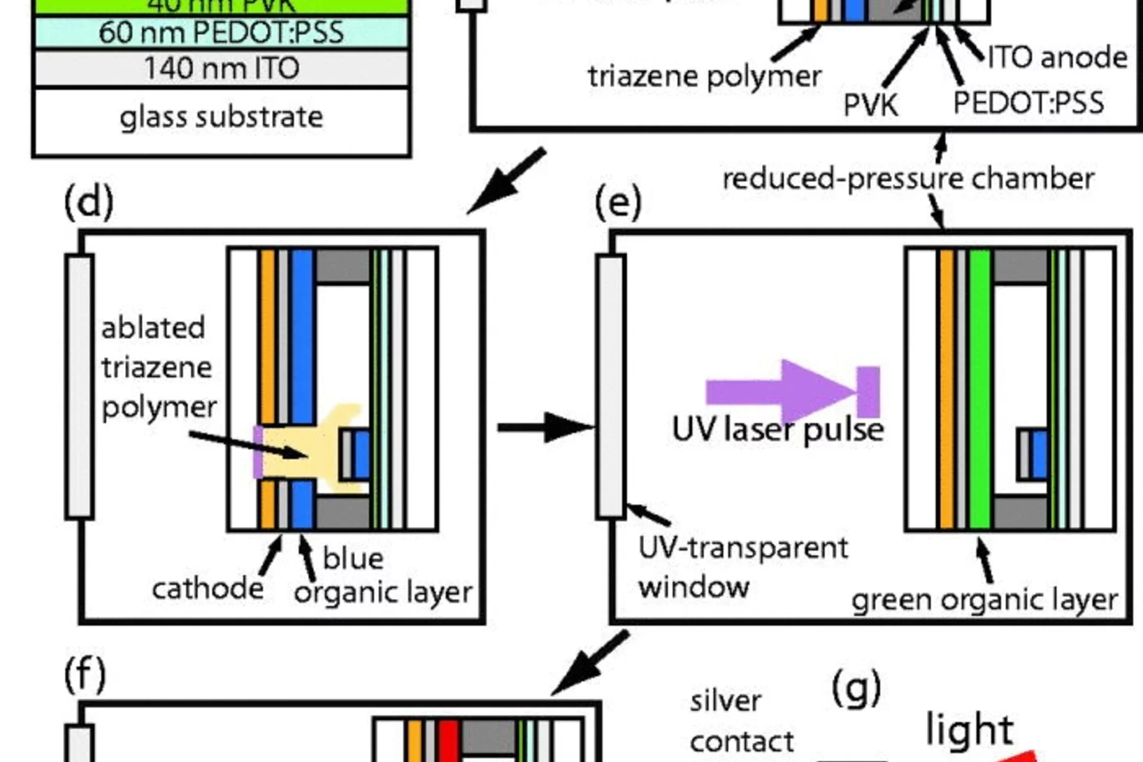
Red-green-blue polymer light-emitting diode pixels printed by optimized laser-induced forward transfer
An optimized laser-induced forward transfer (LIFT) technique has been used to fabricate tri-color organic light-emitting diode (OLED) pixels. At reduced pressures, and with a defined donor-receiver gap, patterned depositions of polyfluorene-based OLED pixels have been achieved. OLED pixel functionality has been demonstrated and compared with devices made using conventional deposition techniques. In addition, improved functionality has been obtained by coating the cathode with an electron-injecting layer, a process not possible using conventional OLED fabrication techniques. The OLED pixels fabricated by LIFT reach efficiencies on the range of conventionally fabricated devices and even surpass them in the case of blue pixels.

![Sketch of a ferroic triangle showing the relation and techniques with which the ferroic orders, FM, AFM, and FE, and their mutual coupling have been established. The experimental techniques written in black letters (polarized neutron reflectometry, PNR; resonant soft x-ray diffraction, SXRD; x-ray diffraction, XRD) to identify ferroic properties have been reported elsewhere [22, 24]. Magnetization, susceptibility, μSR, neutron diffraction, and electrical polarization are reported.](/sites/default/files/styles/teaser_grid_3_2_crop_xl/public/import/num/SHL20160822CoexistingEN/CWS_PRB_94_054423_2016.jpg.webp?itok=lQcJnePQ)
![Temperature dependence of the (050) reflection from a 200 nm o−LuMnO3 [110]-oriented film. Inset (a): Temperature dependence of the integrated intensity from the (050) structural reflection (black) and the (0qb≈½0) magnetic reflection (red) of this film. Inset (b): The simplest approximation for a distortion producing nonzero intensity for a (0k0) reflection with k odd, depicted for two atoms along the b direction.](/sites/default/files/styles/teaser_grid_3_2_crop_xl/public/import/num/SHL20141014MultiferroicPropertiesEN/LMO_Strain_Will_PRL_2014.jpg.webp?itok=HqQwlzeG)
![(a) Mn K-edge XANES spectra of the ∼60 nm o-LMO epitaxial film were measured at room temperature for polarizations E || [110] and E || [001]. The inset shows the magnified pre-edge features. (b) FEFF simulations using the crystallographic data of the bulk o-LMO sample for E || [110] and E || [001]. The simulated pre-edges are shown on a larger scale in the inset.](/sites/default/files/styles/teaser_grid_3_2_crop_xl/public/import/lmx-interfaces/ScientificHighlights2012EN/YI_APL_2012.jpg.webp?itok=EjikdtFC)
