Abstract:
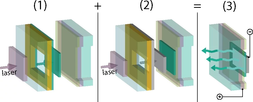
Patterned deposition of polymer light-emitting diode (PLED) pixels is a challenge for electronic display applications. PLEDs have additional problems requiring solvent orthogonality of different materials in adjacent layers. We present the fabrication of a PLED pixel by the sequential deposition of two different layers with laser-induced forward transfer (LIFT), a “dry” deposition technique. This novel use of LIFT has been compared to “normal” LIFT, where all the layers are transferred in a single step, and a conventional PLED fabrication process. For the sequential LIFT, a 50-nm film of an alcohol-soluble polyfluorene (PFN) is transferred onto a receiver with a transparent anode, before an aluminum cathode is transferred on top. Both steps use a triazene polymer dynamic release layer and are performed in a medium vacuum (1 mbar) across a 15 μm gap. The rough morphologies of the single-layer PFN pixels and the PLED device characteristics have been investigated and compared to both bilayer Al/PFN pixels fabricated by normal LIFT and conventionally fabricated devices. The functionality of the sequential LIFT pixels (0.003 cd/A, up to 200 mA/cm2, at 30−40 V) demonstrates the suitability of LIFT for sequential patterned printing of different thin-film layers.
Keywords: Laser induced forward transfere; Laser printing; sequential laser deposition; organic light emitting diodes; triazene polymer; PLED pixels; thin-films; patterned deposition: laser direct-write;
Facility: ENE, EMPA, LMX, Thin Films and Interfaces
Reference: J. R. H. Shaw-Stewart, T. Lippert, M. Nagel, F. A. Nüesch, A. Wokaun; Appl. Mater. & Interfaces 4, 3535 (2012)
Read full article: here
Facility: ENE, EMPA, LMX, Thin Films and Interfaces
Reference: J. R. H. Shaw-Stewart, T. Lippert, M. Nagel, F. A. Nüesch, A. Wokaun; Appl. Mater. & Interfaces 4, 3535 (2012)
Read full article: here

