Rydberg states in Si ∂-layers

Calculated Rydberg wavefunctions
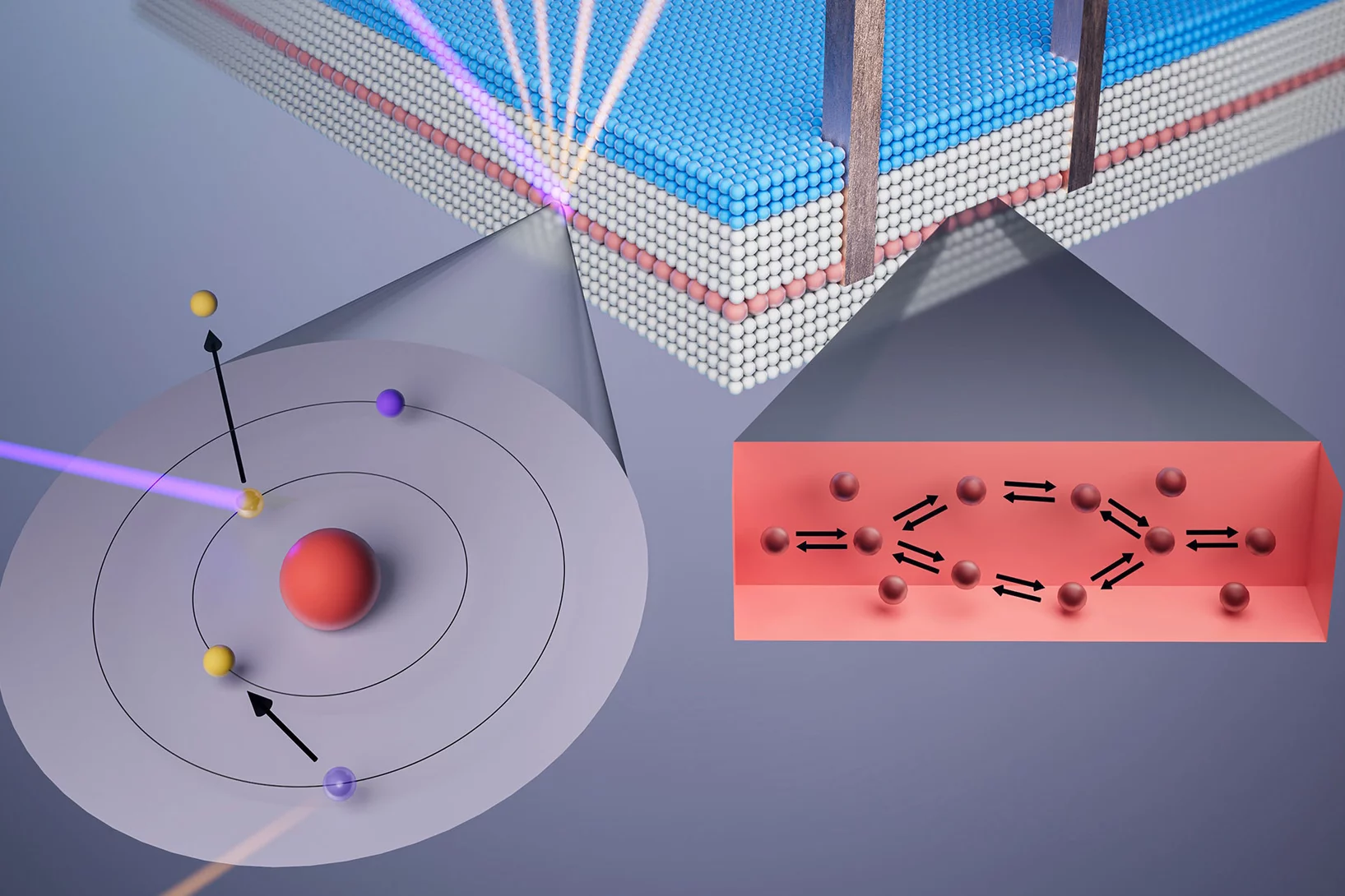
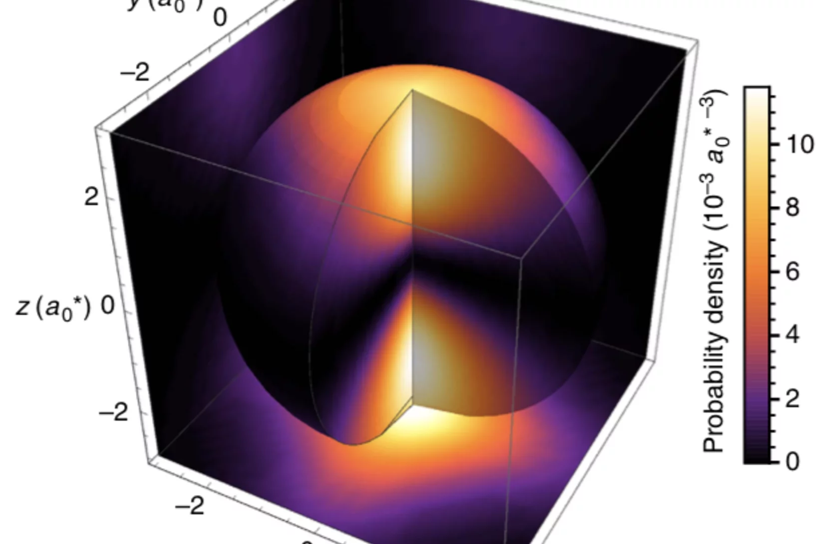
Calculated wavefunctions of Rydberg states in the bulk and near a Si/SiO2/Vacuum interface, as realized in our delta-layer samples.

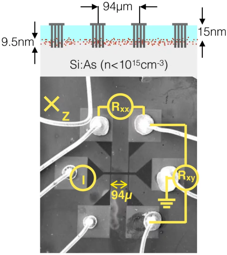
For solid-state quantum computing the ability to deterministically confine donors in a semiconductor is crucial, not only to create quantum bits defined by the electron or nuclear spin of a dopant, but also to fabricate control systems such as gates mediated by one-dimensional wires or two-dimensional “delta” (∂) layers.
In this project low dimensional devices are made by confining group V donors in Si. The devices are then investigated electrically by low temperature magnetoresistance measurements and optically by using techniques such as Fourier transform infra-red (FTIR) spectroscopy and angle resolved photo-emission spectroscopy (ARPES). This allows to understand characteristics of the donor electrons in the Si crystal such as interactions between dopant atoms, the spin-orbit and spin-spin coupling, the metal-insulator transition, and their dependence on dopant species. The goal is to reduce the dimensionality of the confinement to one and zero dimensions and to create ordered single-atom arrays, as well as to measure their quantum electro-optic properties.

Element-specific, non-destructive profiling of layered heterostructures
N. D'Anna, J. Bragg, E. Skoropata, N. Ortiz Hernández, A. G. McConnell, M. Clémence, H. Ueda, P. C. Constantinou, K. Spruce, T. J. Z. Stock, S. Fearn, S. R. Schofield, N. J. Curson, D. Ferreira Sanchez, D. Grolimund, U. Staub, G. Matmon, S. Gerber, G. Aeppli
arXiv:2410.00241

Non-destructive X-ray imaging of patterned delta-layer devices in silicon
N. D'Anna, D. Ferreira Sanchez, G. Matmon, J. Bragg, P. C. Constantinou, T. J.Z. Stock, S. Fearn, S. R. Schofield, N. J. Curson, M. Bartkowiak, Y. Soh, D. Grolimund, S. Gerber, G. Aeppli
Advanced Electronic Materials 2023, 2201212 (2023)

Two- to three-dimensional crossover in a dense electron liquid in silicon
G. Matmon, E. Ginossar, B. J. Villis, A. Kölker, T. Lim, H. Solanki, S. R. Schofield, N. J. Curson, J. Li, B. N. Murdin, A. J. Fisher, G. Aeppli
Phys. Rev. B 97, 155306 (2018)

Coherent superpositions of three states for phosphorous donors in silicon prepared using THz radiation
S. Chick, N. Stavrias, K. Saeedi, B. Redlich, P. T. Greenland, G. Matmon, M. Naftaly, C. R. Pidgeon, G. Aeppli, B. N. Murdin
Nat. Commun. 8, 16038 (2017)


Integrated Circuits

The tiniest secrets of integrated circuits revealed

New research has demonstrated that the secrets of the tiniest active structures in integrated circuits can be revealed using a non-destructive imaging technique. The breakthrough required the efforts of an international team of scientists from JKU and Keysight Technologies (Austria), ETH/EPFL/PSI and IBM Research - Europe (Switzerland) and from UCL (UK).

Giant Multiphoton THz.png

Giant multiphoton absorption points towards new methods for THz quantum control

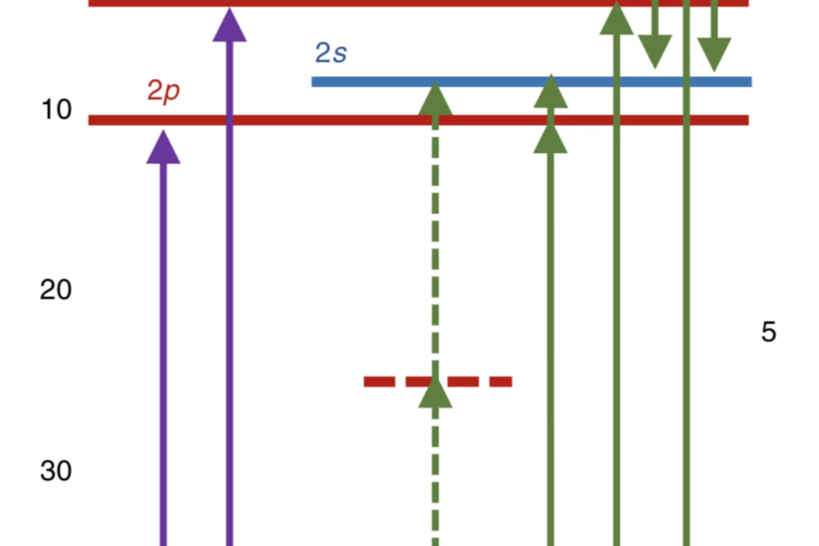
In findings recently published in Nature Photonics, a team including researchers from the UK, the Netherlands and Photon Sciences division head Gabriel Aeppli have investigated multi-photon THz absorption in Si:P. Their studies, using the THz free-electron laser FELIX, discovered a two photon absorption cross-section ten orders of magnitude higher than that of a natural hydrogen atom and may enable new methods in quantum control. In addition to the original publication their findings are also discussed in a 'News and Views' article.

CoherentSuperpositions.png

Coherent superpositions of three states for phosphorous donors in silicon prepared using THz radiation

Superposition of orbital eigenstates is crucial to quantum technology utilizing atoms, such as atomic clocks and quantum computers, and control over the interaction between atoms and their neighbours is an essential ingredient for both gating and readout. A team of researchers including Photon Science division head Gabriel Aeppli has demonstrated THz laser pulse control of Si:P orbitals using multiple orbital state admixtures, observing beat patterns produced by Zeeman splitting. The beats are an observable signature of the ability to control the path of the electron, which implies we can now control the strength and duration of the interaction of the atom with different neighbours. This could simplify surface code networks which require spatially controlled interaction between atoms. The full article can be read in Nature Communications

NonDestructive.png

Nondestructive imaging of atomically thin nanostructures buried in silicon

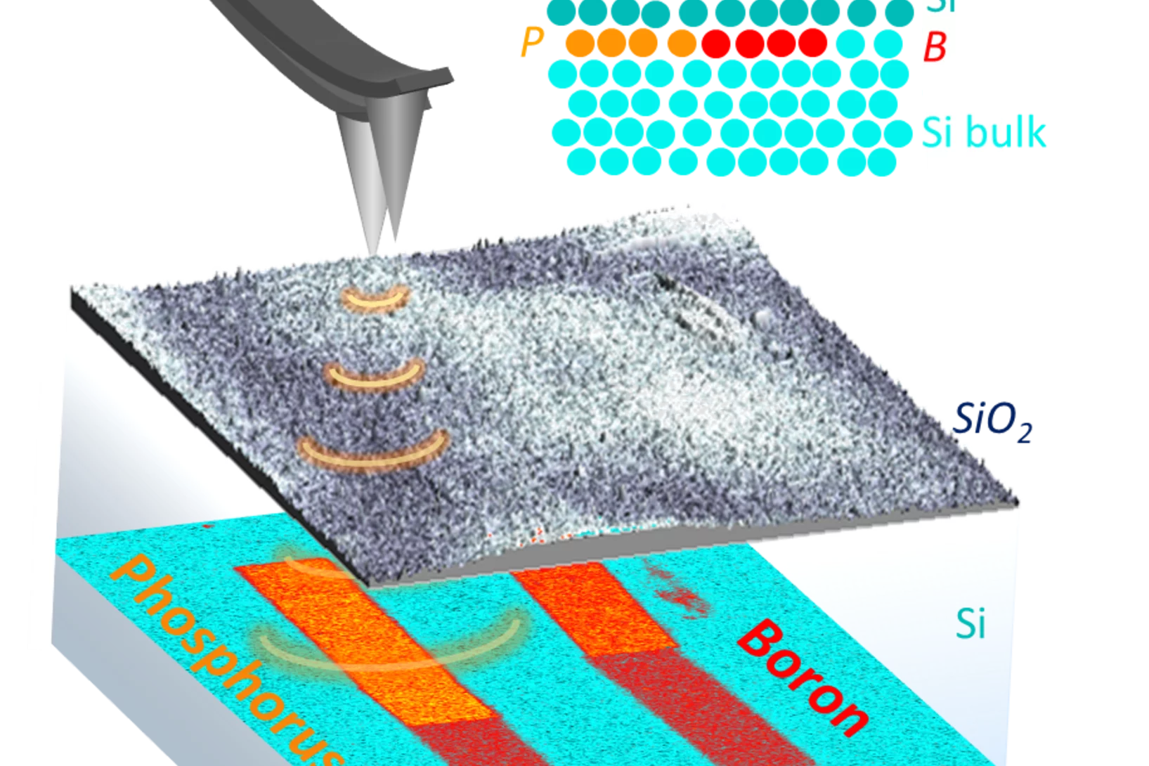
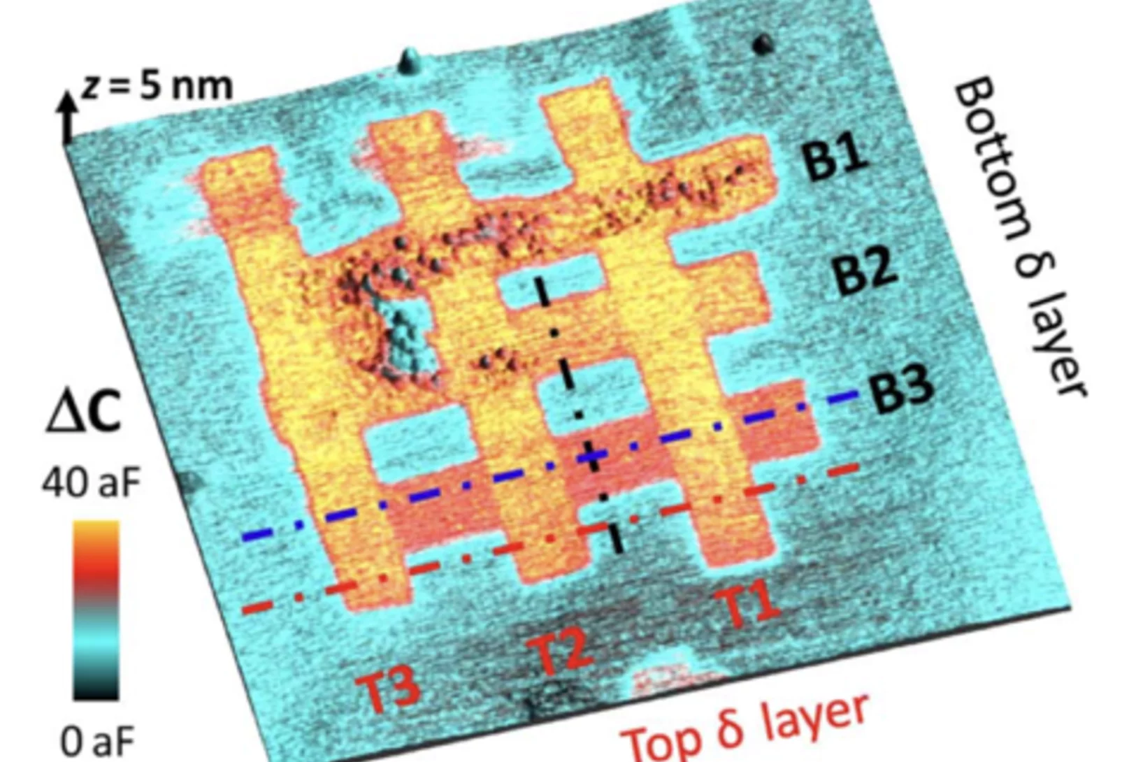
A team of researchers including Photon Sciences division head Gabriel Aeppli have demonstrated the first non-destructive imaging of atomically thin nanostructures in silicon. Such structures are the building blocks of quantum devices for physics research and are likely to serve as key components of devices for next-generation classical and quantum information processing. Until now, the characteristics of buried dopant nanostructures could only be inferred from destructive techniques and/or the performance of the final electronic device; this severely limits engineering and manufacture of real-world devices based on atomic-scale lithography. In work recently published in Science Advances, the team use scanning microwave microscopy (SMM) to image and electronically characterize three-dimensional phosphorus nanostructures fabricated via scanning tunneling microscope based lithography.