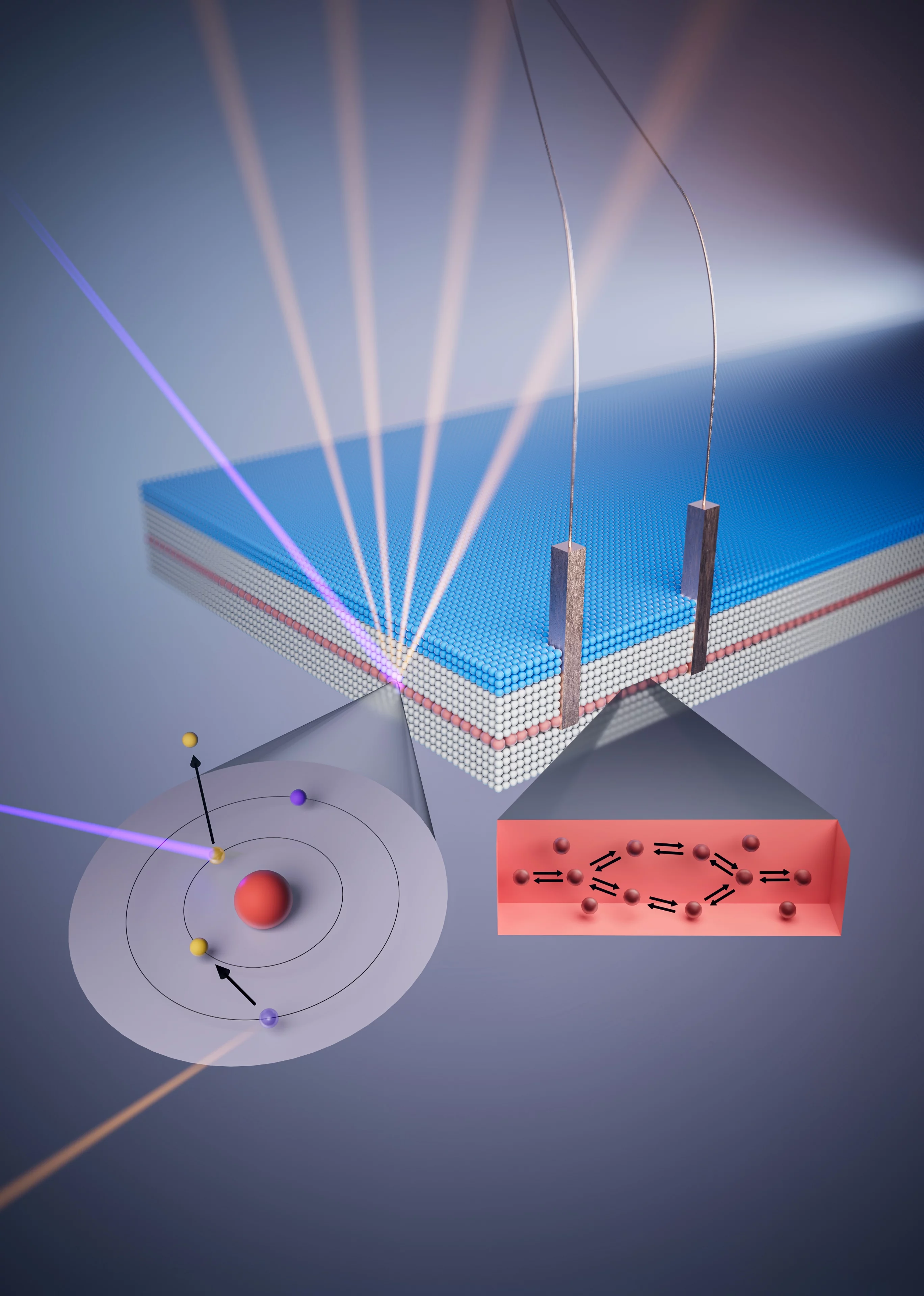
A recent work, published by PSI scientists in collaboration with UCL, demonstrates a technique which will make it possible to image a single atom trapped inside a silicon crystal changing neither its position nor electronic properties. This will be an invaluable tool to further develop transistor technologies and quantum computing.
In the field of integrated silicon electronics, miniaturization has gone a very long way. So far in fact, that we can make structures smaller than we can image without destroying them. For example, it is now possible to deterministically place single dopant atoms inside silicon; this is a feat that Prof. Neil Curson’s group at University College London (UCL) has accomplished with arsenic atoms. The dopant atoms contain more electrons than the surrounding silicon, so lines of dopants can act as wires in an electric circuit. Such circuits, determined by single atoms, will enable the next generation of extremely small transistors and are among the strong candidates to realize quantum computers. While single-atom circuits are poised to be a main player in future technologies, a major hurdle remains before they can be industrially exploited: quality control, or in other words the ability to confirm that the circuit is built to specifications.
Take for example the latest generation smartphones, which contain more than 10 billion transistors. All these transistors need to be fully functional, which cannot be achieved simply by reliable manufacturing. There is also a need for device-level quality control procedures for a phone to work reliably.
But with the current fast pace of transistor miniaturization, quality control has become ever more challenging, a challenge that a team of scientists at the Paul Scherrer Institut PSI has taken up by showing that X-rays from the Swiss Light Source SLS can do just what is needed: In their experiments they obtained a precise image of the dopant atoms buried in silicon and showed that the atoms were unaffected by the measurement.
The demonstration included three main steps. First, the conductivity of a small device containing a 20 x 200 µm2 large two-dimensional dopant layer – roughly a hair’s breadth – buried 30 nm – a thousand times thinner than a hair – below the silicon surface was measured at low temperatures – only some degrees above absolute zero temperature – and in various magnetic fields. These measurements make use of a quantum interference effect of the conductive electrons called weak localization. The interference is very sensitive to externally applied magnetic fields, so that it is possible to determine the thickness of the two-dimensional layer with a precision of 0.2 Angstrom, smaller than the size of an atom.
The second step was to use X-rays from the SLS synchrotron to gently excite the dopant atoms in the device and to detect the fluorescence photons that they emit as they de-excite. As each atom-species emits fluorescence photons with a different energy, it is possible to distinguish the different atoms in the device. The results showed that the signal from as few as a hundred thousand atoms in a 1-µm2 region could be detected this way, and that with the quick progress of synchrotron X-ray sources it will soon be possible do the same with a single atom in a 5-nm2 region.
The third and final step was repeating step one to ensure that the dopant atoms were unaffected by the dose of radiation received during the X-ray measurements. It turned out the X-ray imaging had no measurable effect on the dopant atoms.
With the proof of this non-destructive imaging technique that can be used for quality control of next-generation electronic devices, the work now published in the journal Advanced Electronics Materials represents an important technological development enabled by the close collaboration of scientists at PSI and UCL. Ultimately, the possibility to non-destructively control the quality of fabricated atom-thin devices will foster faster progress towards smaller and more efficient electronics.
Text: Paul Scherrer Institute / Nicolò D'Anna and Simon Gerber
Contact
Dr. Nicolò D'Anna
Department of Physics
University of California San Diego, La Jolla, CA 92093, USA
Email: ndanna@ucsd.edu
Dr. Dario Ferreira Sanchez & Dr. Daniel Grolimund
Laboratory for Synchrotron Radiation and Femtochemistry
Paul Scherrer Institut, 5232 Villigen PSI, Switzerland
Email: dario.ferreira@psi.ch & daniel.grolimund@psi.ch
Prof. Dr. Neil J. Curson
London Centre for Nanotechnology
University College London, London, WC1H 0AH, UK
Email: n.curson@ucl.ac.uk
Dr. Simon Gerber
Laboratory for X-ray Nanoscience and Technologies
Paul Scherrer Institut, 5232 Villigen PSI, Switzerland
Email: simon.gerber@psi.ch
Prof. Dr. Gabriel Aeppli
Photon Science Division
Paul Scherrer Institut, 5232 Villigen PSI, Switzerland
Department of Physics & Quantum Center
Eidgenössische Technische Hochschule Zürich, 8093 Zürich, Switzerland
Institute of Physics
Ecole Polytechnique Fédérale de Lausanne, 1015 Lausanne, Switzerland
Email: gabriel.aeppli@psi.ch
Original Publication
Non-destructive X-ray imaging of patterned delta-layer devices in silicon
N. D'Anna, D. Ferreira Sanchez, G. Matmon, J. Bragg, P.C. Constantinou, T.J.Z. Stock, S. Fearn, S.R. Schofield, N.J. Curson, M. Bartkowiak, Y. Soh, D. Grolimund, S. Gerber, and G. Aeppli
Advanced Electronic Materials 2023, 2201212 (2023)
DOI: 10.1002/aelm.202201212
Further information
Copyright
PSI provides image and/or video material free of charge for media coverage of the content of the above text. Use of this material for other purposes is not permitted. This also includes the transfer of the image and video material into databases as well as sale by third parties.

