
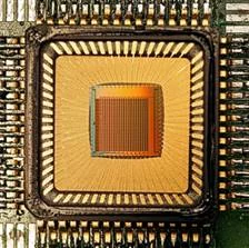
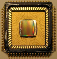
Switched Capacitor Arrays (SCA) are custom made silicon chips which can sample an analog input signal at high speed. After a trigger, the analog signal is then are read out at lower speed, typically in the few MHz regime. SCAs have been used in physics since many years successfully, but mostly chips have been designed for a specific experiment. When the MEG experiment was designed at PSI, it was clear that a SCA chip is required to deal with the pile-up problems anticipated in that experiment. Rather than developing another specialized chip, it has been decided to design a SCA chip which can be used in many different experiments and industrial applications. This chip is now available through the PSI technology transfer program, together with an evaluation board.
DRS1
The Domino Sampling Chip (DSC) was designed by Ch. Broenninam at PSI in 1998 [Ch. Broennimann et al., NIM A420, 264 (1999)]. It had 128 sampling cells running at up to 1.2 GHz and was used in the PIBETA experiment at PSI. Based on this development, the DRS1 chip has been designed in 2001 by Stefan Ritt. It was a single-channel prototype for test purposes only.
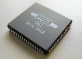
DRS2
The DRS2 chip designed in 2003 had already 10 channels with 1024 bins. It runs at up to 4.5 GHz and is used in the MEG experiment to read 900 channels of PMTs and 3000 channels of drift chamber anodes and cathodes from 2006 to 2008. The nonlinearity and temperature dependence of this chip require extensive calibrations.
DRS3
The DRS3 chip designed in 2006 fixed the temperature dependence by utilizing one operational transient amplifier (OTA) per sampling cell. Its analog bandwidth is 450 MHz (-3 dB). This chip was produced only for prototype studies.
DRS4
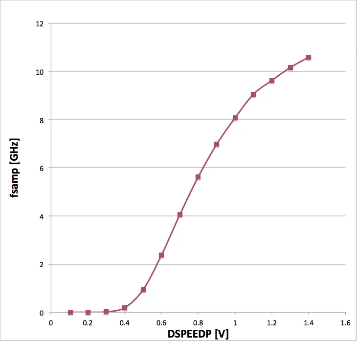
The DRS4 chip designed in 2007 has an increased bandwidth of 950 MHz (-3dB) and fixes a few other flaws of the DRS3. It contains 9 channels each 1024 cells deep, which can be daisy-chained to achieve a virtually unlimited sampling depth. The sampling frequency ranges from 0.7 GSPS to 5 GSPS, while a on-chip PLL stabilizes the sampling frequency with a jitter better than 30 ps. The power requirement is 40 mW per channel or less, depending on the sampling speed. A special readout mode reduces the dead time 30 ns times the number of cells to be read out (for example 3us for a region of 100 cells).
It has been shown that timing measurements with an accuracy of less than four picoseconds are possible with the DRS4 chip.
It has been shown that timing measurements with an accuracy of less than four picoseconds are possible with the DRS4 chip.
DRS5
In 2012, the design of the next generation chip has been started. The design goals are
- Increased analog bandwidth > 3 GHz
- Sampling speed 10 GSPS
- Dead-time less readout mode
- Analog FIFO mode for segment storage
- Internal triggering
- Deeper sampling depth, more channels
A first prototype of the inverter chain in the new 110 nm UMC technology has been designed and successfully tested in January 2013. A sampling speed of 10.6 GSPS has been achieved. First prototypes of this chips are however not expected before 2023.