
Researchers of the Paul Scherrer Institute PSI have made detailed 3-D images of a commercially available computer chip. This marks the first time a non-destructive method has visualized the paths of a chip’s internal wiring (just 45 nanometres — 45 millionths of a millimetre — wide) and its 34-nanometre-high transistors clearly without distortions or deformations. It is a major challenge for manufacturers to determine if, in the end, the structure of their chips conforms to the specifications. Thus these results represent one important application of an X-ray tomography method that the PSI researchers have been developing for several years. In their experiment, the researchers examined a small piece that they had cut out of the chip beforehand. This sample remained undamaged throughout the measurement. The goal now is to extend the method in such a way that it can be used to examine complete chips. The researchers conducted the experiments at the Swiss Light Source SLS of the Paul Scherrer Institute. They report their results in the latest edition of the journal Nature.
The electrical wiring in many of the electronic chips in our computers and mobile phones are just 45 nanometres wide, the transistors 34 nanometres high. While it is standard practice today to produce structures this delicate, it remains a challenge to measure the exact structure of a finished chip in detail in order to check, for example, if it is built according to the specifications. Nowadays, for such examinations, manufacturers mainly use a method in which layer after layer of the chip is removed and then, after each step, the surface is examined with an electron microscope; this is known as FIB/SEM — focused ion beam/scanning electron microscope imaging.
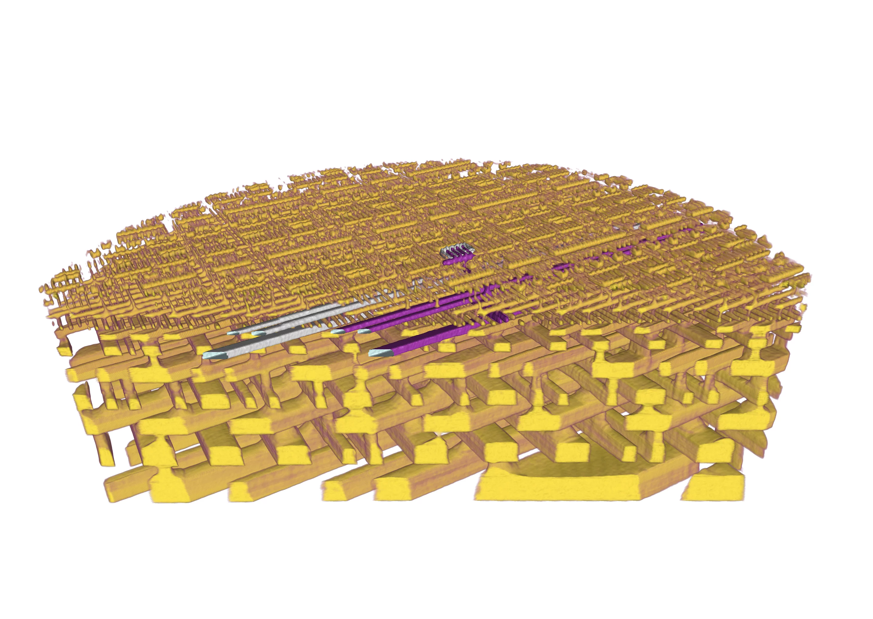
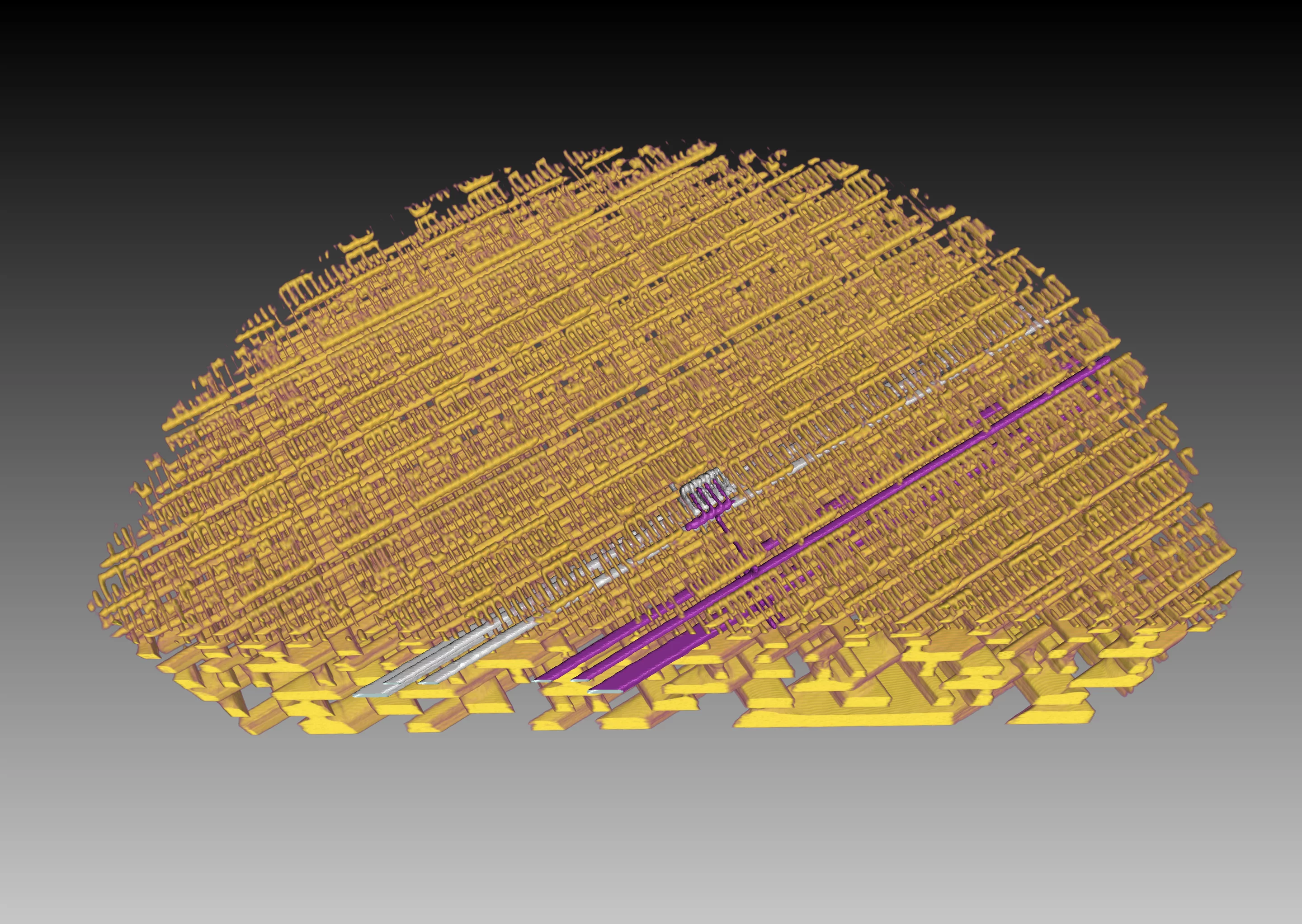
Now researchers of the Paul Scherrer Institute PSI have used X-rays to achieve non-destructive 3-D imaging of a chip, so that the paths of the conducting lines and the positions of the individual transistors and other circuit elements became clearly visible. The image resolution we were able to produce is comparable to the conventional FIB/SEM examination method
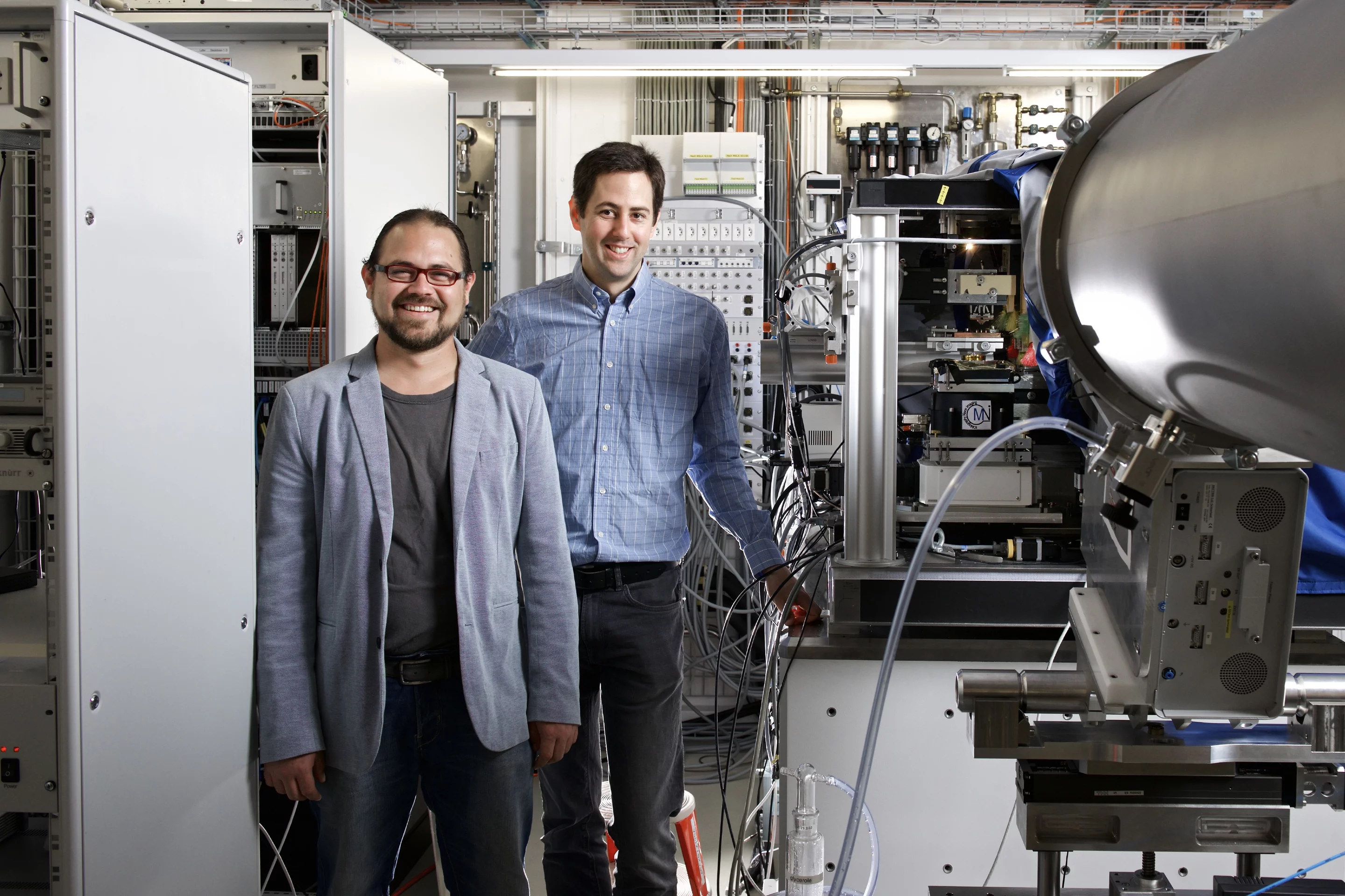
, explains Mirko Holler, leader of the project. But we were able to avoid two significant disadvantages: Firstly, the sample remained undamaged, and we have complete information about the three-dimensional structure. Secondly, we avoided distortions of the images that arise in FIB/SEM if the surface of the individual slice is not exactly planar.
Positioned with nanometre precision
For their study, the researchers used a special tomographic method (ptychotomography) that they have developed and enhanced over the course of recent years, and which today offers the worldwide best resolution of 15 nanometres (15 millionths of a millimetre) for examination of a comparably large volume. In the experiment the object to be studied is X-rayed at precisely determined places with light from the Swiss Light Source SLS of the Paul Scherrer Institute — for each illuminated spot a detector then measures the X-ray light pattern after its passage through the sample. The sample is then rotated in small steps and then X-rayed again step-wise after each turn. From the whole set of data obtained, the three-dimensional structure of the sample can be determined. With these measurements, the position of the sample must be known to a precision of just a few nanometres — that was one of the particular challenges in setting up our experimental station
, Holler says.
In their experiment the researchers examined small pieces of two chips — a detector chip developed at PSI and a commercially available computer chip. Each piece was about 10 micrometres (that is, 10 thousandths of a millimetre) in size. While the examination of an entire chip with the present measurement setup is not possible, the method’s advantages are brought to bear even in this form, so that the first prospective users have already expressed an interest in conducting measurements at PSI.
Video
The goal: to examine entire microchips
We are currently starting to extend the method in such a way that it can be used to examine entire microchips within an acceptable measurement time. Then it will also be possible to study the same area of a chip multiple times, for example to observe how it changes under external influences
, explains Gabriel Aeppli, head of the Synchrotron Radiation and Nanotechnology Division at the PSI.
Text: Paul Scherrer Institute/Paul Piwnicki
About PSI
The Paul Scherrer Institute PSI develops, builds and operates large, complex research facilities and makes them available to the national and international research community. The institute's own key research priorities are in the fields of matter and materials, energy and environment and human health. PSI is committed to the training of future generations. Therefore about one quarter of our staff are post-docs, post-graduates or apprentices. Altogether PSI employs 2000 people, thus being the largest research institute in Switzerland. The annual budget amounts to approximately CHF 370 million. PSI is part of the ETH Domain, with the other members being the two Swiss Federal Institutes of Technology, ETH Zurich and EPFL Lausanne, as well as Eawag (Swiss Federal Institute of Aquatic Science and Technology), Empa (Swiss Federal Laboratories for Materials Science and Technology) and WSL (Swiss Federal Institute for Forest, Snow and Landscape Research).
(Last updated in May 2016)
Additional information
Detailed article on the method used
Contact
Dr. Mirko HollerLaboratory for Macromolecules and Bioimaging, Research Division Synchrotron Radiation and Nanotechnology
Paul Scherrer Institute, 5232 Villigen PSI, Switzerland
Telephone: +41 56 310 36 13, e-mail: mirko.holler@psi.ch
Original Publication
High-resolution non-destructive three-dimensional imaging of integrated circuitsMirko Holler, Manuel Guizar-Sicairos, Esther H. R. Tsai, Roberto Dinapoli, Elisabeth Müller, Oliver Bunk, Jörg Raabe, Gabriel Aeppli
Nature 16 March 2017
DOI: 10.1038/nature21698