
A recent breakthrough by researchers at the Swiss Nanoscience Institute sees for the first time the creation of thin films with controllable electronic properties. This discovery could have a large impact on future applications in sensors and computing. The international collaboration of researchers from the Universities of Basel and Heidelberg and the Paul Scherrer Institute have published the work in the prestigious scientific journal Science.
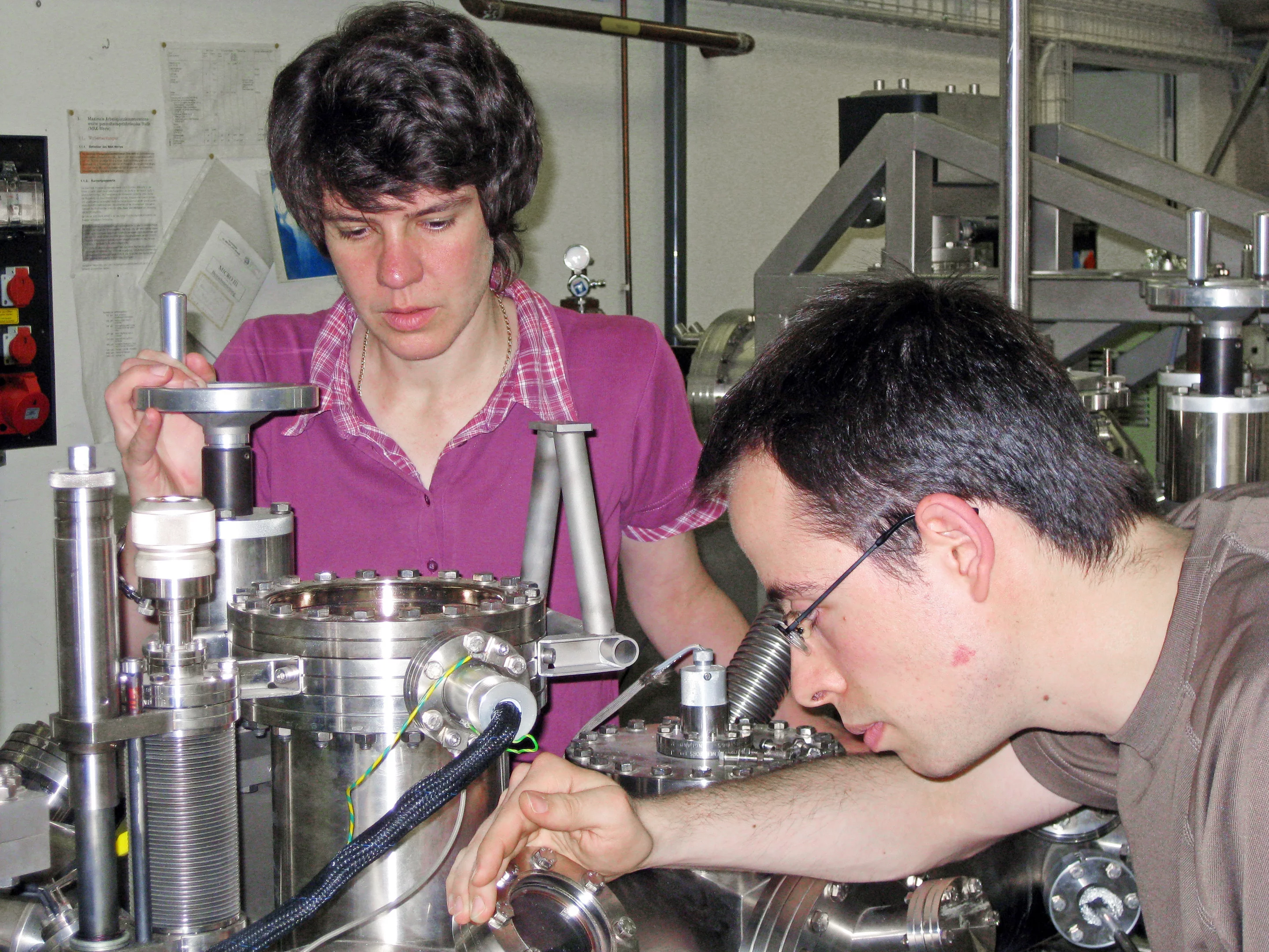
It's commonly accepted that electrical resistance of a given material cannot be adjusted as is the case with, for example, density and color. However, Dr Meike Stöhr and her collaborators have now succeeded in developing a new method to selectively tune surface properties such as resistance.
The interdisciplinary team of physicists and chemists have developed a substance which, after heating on a copper surface, exhibits a two dimensional network with nanometer sized pores. The interaction of this network with the existing electron gas on the metal surface leads to the following effect: the electrons underneath the network are pushed into the pores to form small bunches of electrons called quantum dots.
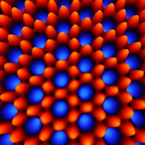
electronic metamaterialis generated by supramolecular selfassembly on a metal surface. The periodic influence of the porous molecular network on the otherwise free-electron-like surface state results in the formation of an electronic band.
Great potential for materials research
By varying parameters such as the height and diameter of the pores the possibility arises to selectively tune the properties of the material. Further possibilities arise from the ability to fill the pores with different molecules. This allows direct access to the properties of the material which are dependent on the electronic structure, such as conductivity, reflectivity and surface catalysis properties. This will lead to the emergence of new materials with adjustable electronic properties.
The underlying physical mechanisms can best be understood by a comparison of the electron-gas with waves in water. Waves on a water surface are reflected by any obstacle they meet. If the obstacle on the surface in question resembles a honeycomb structure, standing waves are set up in each cell of the honeycomb. This then leads to a wave pattern representative of the honeycomb structure of the same size and shape. Applying this analogy to the electron gas, we see that the interaction of the network structure with the electron gas on the metal surface confines the electrons giving rise to a characteristic electron wave structure of the new material.
says Stöhr.
These pore networks are good candidates for new meta-materials. These are man-made materials which, due to their period architecture, have specific optical and electronic properties not found in nature. These properties can be tuned by changing the properties of their component materials. In the case of pore networks, it is the electronic surface properties which can be tuned by careful selection of the nano-pores.
The University of Basel and the Paul Scherrer Institute are long-term partners of the Swiss Nanoscience Institute (SNI), which is also financed by the Canton of Aargau. The SNI also includes both the Nationaler Forschungsschwerpunkt Nanowissenschaften which was founded in 2001, and the Argovia-Netzwerk, founded in 2006 and also financed by the Canton of Aargau. A key partner in this project was the Swiss Light Source of the Paul Scherrer institute.
Contact
Original Publication
-
Lobo-Checa J, Matena M, Müller K, Dil JH, Meier F, Gade LH, et al.
Band formation from coupled quantum dots formed by a nanoporous network on a copper surface
Science. 2009; 325(5938): 300-303. https://doi.org/10.1126/science.1175141
DORA PSI
Further Information
About PSI
The Paul Scherrer Institute PSI develops, builds and operates large, complex research facilities and makes them available to the national and international research community. The institute's own key research priorities are in the fields of future technologies, energy and climate, health innovation and fundamentals of nature. PSI is committed to the training of future generations. Therefore about one quarter of our staff are post-docs, post-graduates or apprentices. Altogether PSI employs 2300 people, thus being the largest research institute in Switzerland. The annual budget amounts to approximately CHF 450 million. PSI is part of the ETH Domain, with the other members being the two Swiss Federal Institutes of Technology, ETH Zurich and EPFL Lausanne, as well as Eawag (Swiss Federal Institute of Aquatic Science and Technology), Empa (Swiss Federal Laboratories for Materials Science and Technology) and WSL (Swiss Federal Institute for Forest, Snow and Landscape Research). (Last updated in June 2025)