
Scientists at the Paul Scherrer Institute and ETH Zurich (Switzerland) have created 3D images of tiny objects showing details down to 25 nanometres (1 nanometre = 1 millionth of a millimetre). In addition to the shape, the scientists determined how particular chemical elements were distributed in their sample and whether these elements were in a chemical compound or in their pure state.
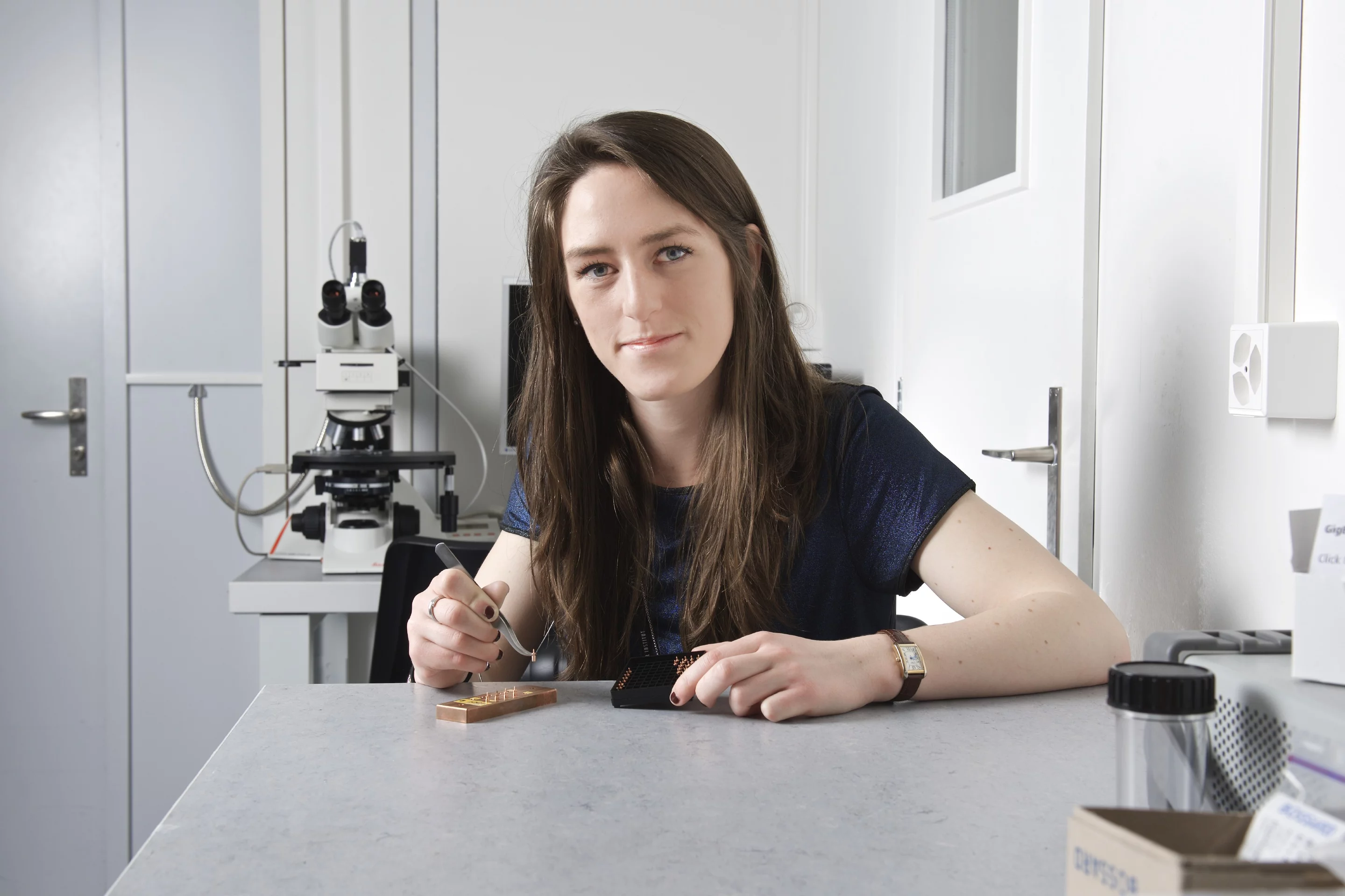
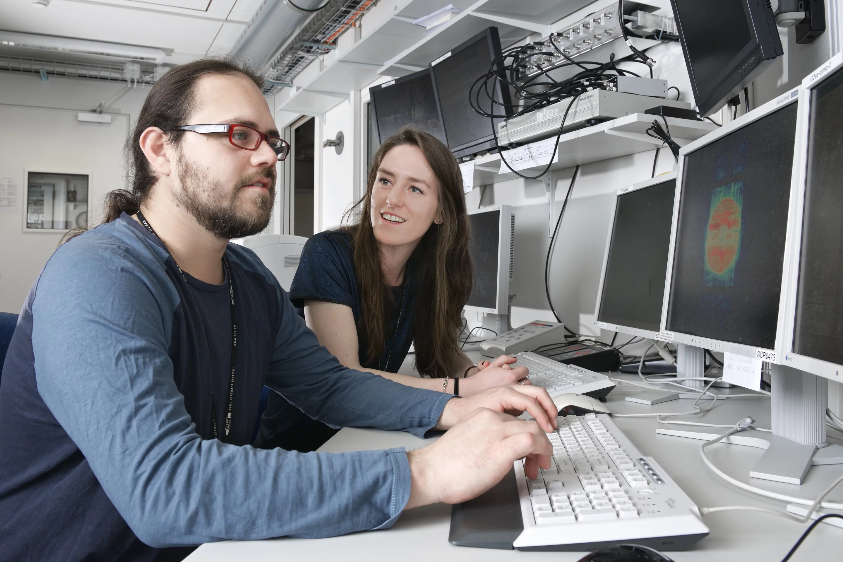
The measurements were performed at the Swiss Light Source at the Paul Scherrer Institute using a method called phase tomography. As in other types of tomography, here x-rays are shone through the sample from different directions to give images from many perspectives. These images are combined using a computer program to give a 3D image.
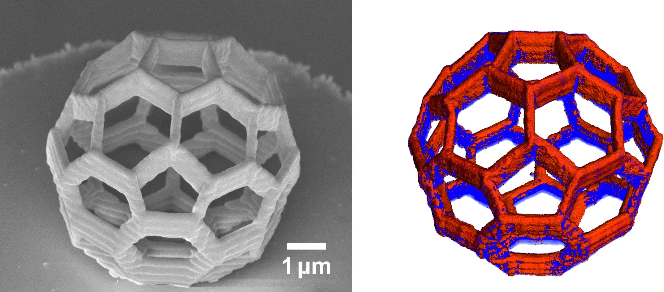
The method was demonstrated using a football-like structure called a buckyball
, only 6 thousandths of a millimetre across, which was fabricated with the latest 3D laser technology. In addition to showing the shape of the object, the method allowed the scientists to pinpoint the locations of a specific chemical element (Cobalt) and deduce further information on the environment of its atoms. They made use of the fact that different elements interact differently with light of different energies, like different colours in visible light, allowing them to see the distribution of a specific element within the sample.
Being able to distinguish different elements and their compounds on the nanometre scale in three dimensions is highly relevant in the development of novel electronic and magnetic parts or more efficient catalysts for the chemical industry.
Text: Paul Scherrer Institut/Paul Piwnicki
About PSI
The Paul Scherrer Institute PSI develops, builds and operates large, complex research facilities and makes them available to the national and international research community. The institute's own key research priorities are in the fields of matter and materials, energy and environment and human health. PSI is committed to the training of future generations. Therefore about one quarter of our staff are post-docs, post-graduates or apprentices. Altogether PSI employs 1900 people, thus being the largest research institute in Switzerland. The annual budget amounts to approximately CHF 350 million.
Contact
Dr. Manuel Guizar-Sicairos, Swiss Light SourcePaul Scherrer Institut, 5232 Villigen PSI, Switzerland (English, Spanish)
Telephone: +41 56 310 3409, E-mail: manuel.guizar-sicairos@psi.ch
Dr. Jörg Raabe, Swiss Light Source
Paul Scherrer Institut, 5232 Villigen PSI, Switzerland (German, English)
Telephone: +41 56 310 5193, E-mail: joerg.raabe@psi.ch
Prof. Dr. Laura Heyderman
Laboratory for Mesoscopic Systems, Department of Materials, ETH Zurich
Laboratory for Micro- and Nanotechnology, Paul Scherrer Institute
5232 Villigen PSI; Switzerland (German, English)
Telephone: +41 56 310 2613; E-Mail: laura.heyderman@psi.ch
Original Publication
Element-Specific X-Ray Phase Tomography of 3D Structures at the NanoscaleClaire Donnelly, Manuel Guizar-Sicairos, Valerio Scagnoli, Mirko Holler, Thomas Huthwelker,
Andreas Menzel, Ismo Vartiainen, Elisabeth Müller, Eugenie Kirk, Sebastian Gliga, Jörg Raabe, and Laura J. Heyderman.,
Phys. Rev. Lett. 114, 115501 (2015);
DOI: 10.1103/PhysRevLett.114.115501; Published: 20 March 2015