
New method allows important insights into polymer semiconductors
Semiconductors made from polymer materials are becoming increasingly important for the electronics industry – as a basis for transistors, solar cells or LEDs – showing important advantages when compared to conventional materials: they are lightweight, flexible and very cheap to produce. Usually, they consist of more than one substance as they get their particular electric properties only when several materials are blended. But in order to find the optimal material, one has to know how different polymers mix together (or don’t) and how the various components contribute to the properties of the material. Researchers from the Paul Scherrer Institute (Switzerland) and the University of Cambridge (United Kingdom) have developed a method that allows them to determine the detailed structure of the material – both in the bulk and on the surface. The investigations were performed at the Swiss Light Source SLS of the Paul Scherrer Institute.
Semiconductors are the basis of most electronic components. Until recently, when speaking about semiconductors, one would think of brittle materials such as silicon, but now a new kind of material might conquer the world of electronics – conjugated polymer semiconductors, i.e. special plastics that can conduct electricity. Electronic devices utilising these materials will usually require not just a single kind of plastic, but rather a variety of materials blended together. The blending of two semiconducting polymers sometimes enables you to achieve properties or function that cannot be achieved with one polymer alone
says Chris McNeill of the University of Cambridge. For example, the efficiency of polymer solar cells and LEDs are greatly improved through blending
. His colleague Benjamin Watts from the Paul Scherrer Institute adds Making electronic devices out of polymer blends is especially difficult because not only do we not understand how the materials operate, it is also very difficult to see the structures that polymer blends tend to form because all polymers look very similar.
We can distinguish between polymer materials that otherwise appear nearly identical
McNeill and Watts have now developed a technique that allows them to distinguish between different polymers within a blend – and they can do so both in the bulk and on the surface of the material. This is very important for polymer-based electronic devices because while the
the scientists explain.work
is done in the bulk of the film, the surface connects the device to other components and the outside world
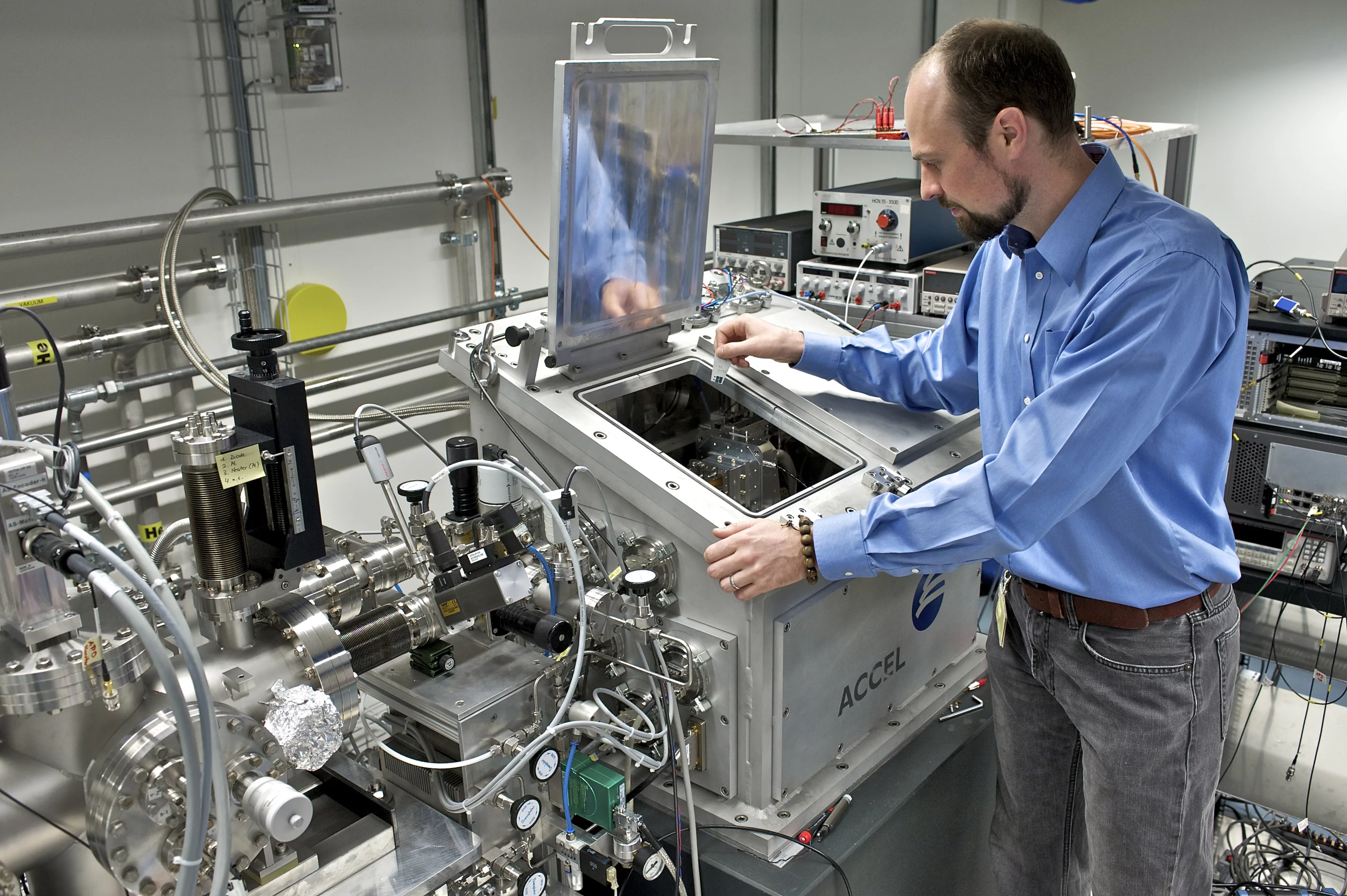
They performed their investigations using synchrotron light at the Swiss Light Source SLS of the Paul Scherrer Institute. Synchrotron light is powerful X-ray light produced by very fast electrons forced to follow a bent path that is much more brilliant than radiation coming out of an ordinary X-ray tube. At the Swiss Light Source synchrotron light is generated by electrons travelling almost at the speed of light on a circular trajectory with a circumference of 288 meters. In their experiments, Watts and McNeill employ the fact that the energy of the light, i.e. the colour, can be adjusted very exactly to highlight subtle differences between the materials investigated. We illuminate our sample with X-ray light that is
tuned
to the carbon atom and so materials that contain carbon atoms (like polymers) absorb much more of the light than one would otherwise expect. This absorption is also very sensitive to the way in which the atoms are linked together, causing materials with different molecular structure to have very different colours
. Thus the X-ray light lets us distinguish between polymer materials that otherwise appear nearly identical.
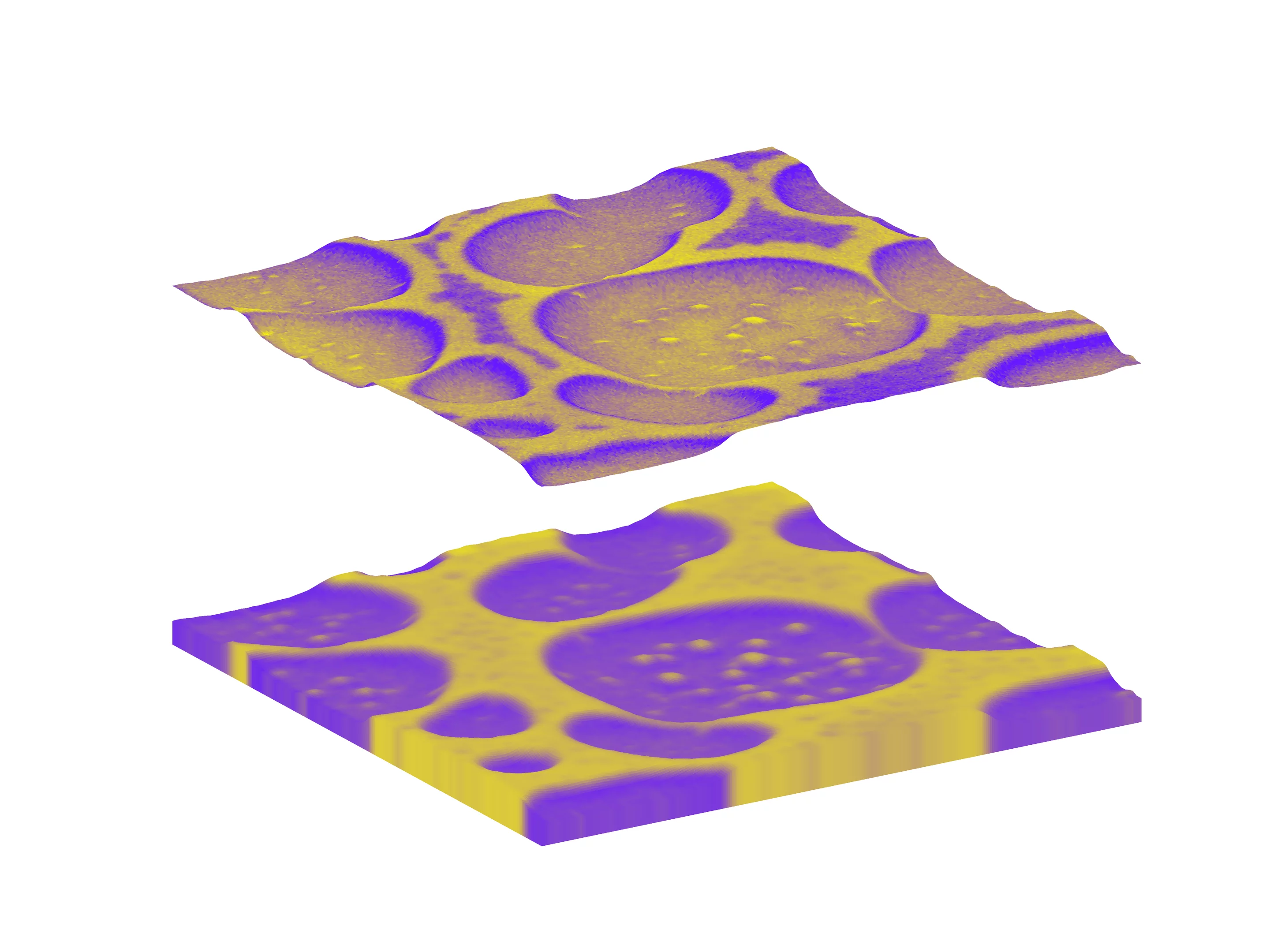
Investigating bulk and surface at the same time
In our experiment we used two very different methods to view the inside bulk and the outer surface of the sample material. To see the inner bulk, we essentially held it up to the light and looked at what
Explains Watts.colours
of x-ray light shone through. To see the outer surface, we had to use a slightly more complicated trick. When an atom absorbs an x-ray, it doesn't like to keep the extra energy and so it gets rid of the energy by spitting out one of its electrons. Now an electron doesn't like moving around outside of an atom and so will grab onto the next atom it comes across, but the electrons spat out of atoms that lie on the surface of the sample material don't have any other atoms to grab onto, just the vacuum that we do the experiment in. Therefore, by observing the electrons coming out of the sample, we get a measure of what X-ray colour
the sample is just on the very surface, where the electrons manage to escape from.
From mobile phone displays to organic solar cells
When asked about the practical impact of his work, Watts explains Organic electronic devices are already becoming available to consumers, in the displays of some mobile phones for instance. Our work will help researchers find ways to make these devices more efficient and more effective. In the example of the mobile phone display, this means that the display can be made brighter and consume less power.
And McNeill adds This research will also help other types of devices come to market such as organic solar cells and devices based on organic field-effect transistors.
About PSI
The Paul Scherrer Institute develops, builds and operates large-scale, complex research facilities, and makes these facilities available to the national and international research community. The Institute’s own research focuses on solid-state physics and the materials sciences, elementary particle physics, biology and medicine, as well as research involving energy and the environment. With a workforce of 1300 and an annual budget of about 260 million CHF, PSI is the largest research institution in Switzerland.
Contact
Dr. Benjamin Watts, Laboratory for Condensed Matter Research, Division Synchrotron Radiation and Nanotechnology,Paul Scherrer Institute, 5232 Villigen PSI, Switzerland,
E-Mail: benjamin.watts@psi.ch, Phone: +41 56 310 5516 (English)
Dr. Christiopher R. McNeill, Cavendish Laboratory,
University of Cambridge, Cambridge CB3 0HE, United Kingdom,
E-Mail: crm51@cam.ac.uk; Phone: +44 1223 337287 (English)
Dr. Jörg Raabe, Laboratory for Condensed Matter Research, Division Synchrotron Radiation and Nanotechnology,
Paul Scherrer Institute, 5232 Villigen PSI, Switzerland,
E-Mail: joerg.raabe@psi.ch, +41 56 310 5193 (Deutsch, English)
Original publication
Simultaneous Surface and Bulk Imaging of Polymer Blends with X-ray SpectromicroscopyBenjamin Watts, Christopher R. McNeill;
Macromolecular Rapid Communications, 2010, DOI: 10.1002/marc.201000269
Images