
Germanium-tin semiconductor lasers can be applied directly to silicon chips
Tiny lasers incorporated into silicon computer chips should speed up the communication inside the chips and between various computer components in future. Experts spent a long time searching for a suitable laser material that is compatible with the silicon chip production process. Scientists from Forschungszentrum Jülich, the Paul Scherrer Institute PSI have now made a major breakthrough. Together with partners from other countries, they present in the journal Nature Photonics a germanium-tin laser that can be applied directly to silicon. It forms a new basis for transferring data on computer chips and sensors using light: faster and using only a fraction of the energy that a classic copper wire requires.
The transfer of data between different processor cores in a single chip as well as between logic elements and memory cells is regarded as a bottleneck in the fast-developing computer technology. Data transmission via light could be the answer to the call for a faster and more energy efficient data flow on computer chips as well as between different board components. Signal transmission via copper wires limits the development of larger and faster computers due to the thermal load and the limited bandwidth of copper wires. The clock signal alone synchronizing the circuits uses up to 30% of the energy – energy which can be saved through optical transmission
, explains Detlev Grützmacher, Director at Jülich's Peter Grünberg Institute.
Some long-distance telecommunication networks and computing centres have been making use of optical connections for decades. These allow very high bandwidths even over long distances. Through optical fibres, signal propagation is almost lossless and possible across various wavelengths simultaneously – a speed advantage which increasingly benefits both micro- and nanoelectronics. The integration of optical components is already well advanced in many areas. However, in spite of intensive research, a laser source that is compatible with the manufacturing of chips has not been achieved up to now
, sais Grützmacher.
Laser material suitable for silicon chips
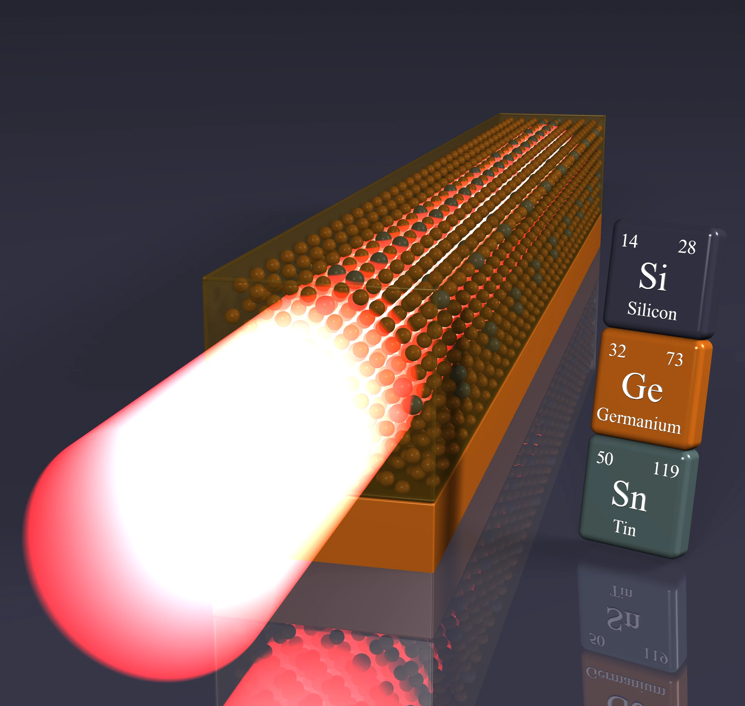
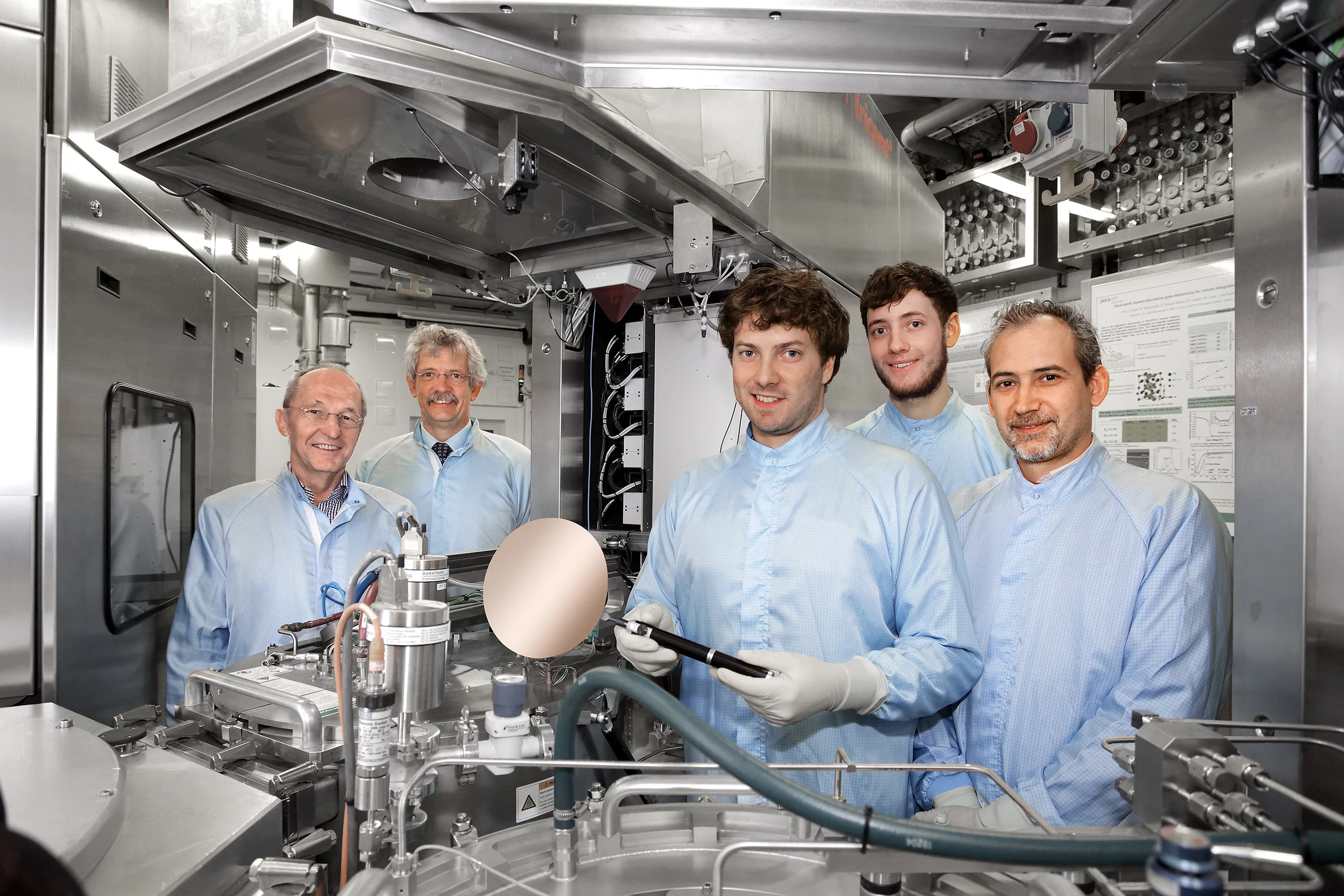
Now, for the first time, the scientists from Jülich’s Peter Grünberg Institute have succeeded in producing a suitable laser by combining germanium and tin The high tin content is decisive for the optical properties. For the first time, we were able to introduce more then ten per cent tin into the crystal lattice without it losing its optical quality
, reports doctoral student Stephan Wirths.
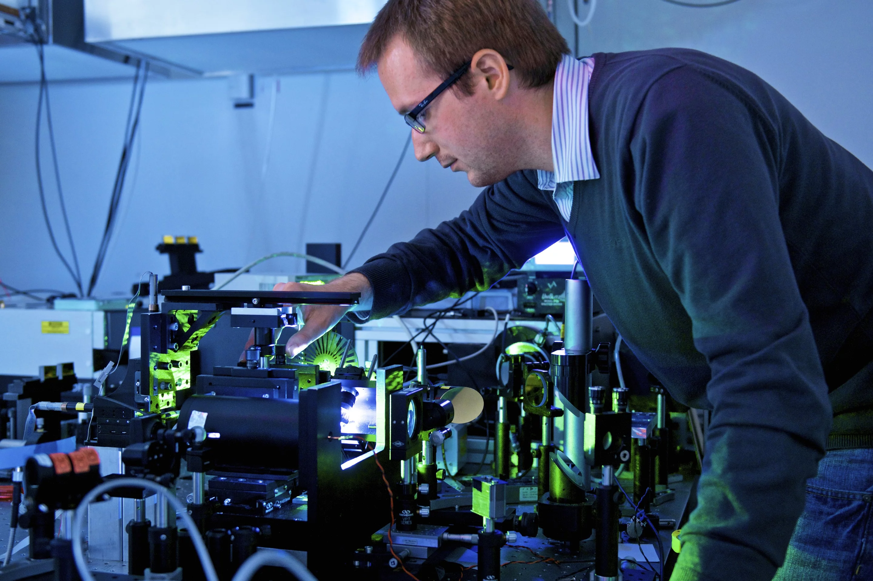
Richard Geiger, a doctoral student at the Laboratory of Micro and Nanotechnology at Paul Scherrer Institute PSI, manufactured the laser structures and measured them with Wirths at PSI. This enabled us to demonstrate that the germanium-tin compound can amplify optical signals as well as generate laser light
, sais Hans Sigg, Head of PSI’s Laboratory of Micro and Nanotechnology. For years, Sigg’s group has been developing materials that might be suitable for lasers in microchips and devising the methods necessary to study these materials.
In the experiment, the material was still stimulated by another laser. The major goal will be to generate laser light with electricity – and ideally without any cooling. The functioning of the laser is so far limited to low temperatures of up to minus 183 degrees Celsius, however. This is mainly due to the fact that we worked with a test system that was not further optimized
, adds Dan Buca from Forschungszentrum Jülich.
Laser component for new applications
The laser beam is not visible to the naked eye, since its wavelength is in the infrared range. This has the advantage that it can be used to detect many carbon compounds. Along with computer chips, completely new applications that have not been pursued so far for financial reasons may thus benefit from the new laser material. Gas sensors or implantable chips for medical applications which can gather information about blood sugar levels or other parameters via spectroscopic analysis are examples. In the future, cost-effective, portable sensor technology – which may be integrated into a smart phone – could supply real-time data on the distribution of substances in the air or the ground and thus contribute to a better understanding of weather and climate development.
Background
The main group is the key
Typical semiconductor lasers for telecommunication systems, made of gallium arsenide for example, however, are costly and consist of elements from main groups three or five. This has profound consequences on the crystal properties. Such laser components cannot therefore be applied directly onto silicon. They have to be produced externally at great effort and subsequently glued to the silicon wafer. However, the lifetime of this kind of component is greatly reduced due to the fact that the thermal expansion coefficients of these elements are significantly different from that of silicon.
In contrast, semiconductors of main group four – to which both silicon and germanium belong – can be integrated into the manufacturing process without any major difficulties. Neither element is very efficient as a light source, however. They are classed among the indirect semiconductors. In contrast to direct semiconductors, they emit mostly heat and only a little light when excited. That is why research groups all over the globe are intensively pursuing the objective of manipulating the material properties of germanium so that it would be able to amplify optical signals and thus make it a usable laser source.
Text: On the basis of a press release by Forschungszentrum Jülich
About PSI
The Paul Scherrer Institute PSI develops, builds and operates large, complex research facilities and makes them available to the national and international research community. The institute's own key research priorities are in the fields of matter and materials, energy and environment and human health. PSI is committed to the training of future generations. Therefore about one quarter of our staff are post-docs, post-graduates or apprentices. Altogether PSI employs 1900 people, thus being the largest research institute in Switzerland. The annual budget amounts to approximately CHF 380 million.
(Last updated in April 2015)
Funding
This project was co-financed by the Swiss National Science Foundation (SNSF), the EU’s 7th EU Framework Programme for Research, and the German Federal Ministry of Education and Research’s project UltraLowPow.
Additional information
Laboratory of Micro and Nanotechnology, Department of Nanospectroscopy, Paul Scherrer Institute:http://www.psi.ch/lmn/nanospectroscopy
Research at the Peter Grünberg Institute, Semiconductor Nanoelectronics (PGI-9):
http://www.fz-juelich.de/pgi/pgi-9/DE/Home/home_node.html
Press release by Forschungszentrum Jülich:
http://www.fz-juelich.de/SharedDocs/Pressemitteilungen/UK/EN/2015/15-01-19gesn-laser.html
Contact
Professor Detlev Grützmacher, Director of the Peter Grünberg Institute, Semiconductor Nanoelectronics, Forschungszentrum Jülich (PGI-9), 52425 Jülich, Germany,tel.: +49 2461 61-2340, e-mail: d.gruetzmacher@fz-juelich.de
Dr. Hans Sigg, Laboratory of Micro and Nanotechnology; Paul Scherrer Institute,
tel.: +41 56 310 40 48, e-mail: hans.sigg@psi.ch
Original Publication
Lasing in direct bandgap GeSn alloy grown on Si (001)S. Wirths, R. Geiger, N. von den Driesch, G. Mussler, T. Stoica, S. Mantl, Z. Ikonic, M. Luysberg, S. Chiussi, J.M. Hartmann, H. Sigg, J.Faist, D. Buca and D. Grützmacher
Nature Photonics (published online 19 January 2015),
DOI: 10.1038/nphoton.2014.321