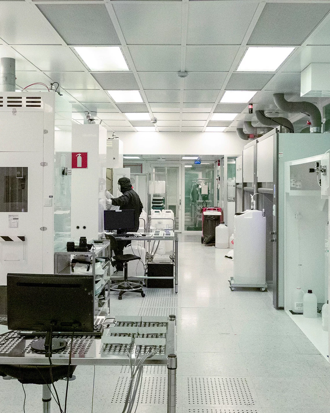
The Paul Scherrer Institute PSI and the Finnish company PiBond to collaborate in the commercialization of advanced EUV semiconductor lithography products.
PiBond Ltd, a leading manufacturer of advanced materials for the semiconductor industry, and Paul Scherrer Institute PSI, the largest research institute for natural and engineering sciences in Switzerland, have signed a technology licensing agreement and strategic collaboration to advance the development of next-generation lithographic materials and drive future semiconductor innovation.
Lithography has been a cornerstone in driving over five decades of unprecedented advancements in semiconductor technology, playing a pivotal role in the next generation of semiconductor integrated circuits. This process technology, particularly in its most advanced form – extreme ultraviolet lithography or EUV – stands as the paragon of ultra-high-precision manufacturing. It is instrumental in fabricating semiconductor chips that are not only faster but also more energy-efficient, fuelling the rapid evolution of artificial intelligence. Currently, development is hampered by limitations in lithographic materials. PiBond is at the forefront, addressing these challenges.
Strategic Cooperation
The aim of this strategic collaboration between PiBond and PSI is to commercialise and deploy novel resist technology in the most advanced semiconductor device manufacturing, and to demonstrate the potential of academic research to drive commercial device innovation.
In addition, this collaboration will pave the way for significant advances in semiconductor technology, providing solutions to pressing industry needs and opening new opportunities for future development.
As part of this agreement, PiBond has established a subsidiary in Switzerland (at Switzerland Innovation Park Innovaare) to further deepen its collaboration with PSI and its research infrastructure. In addition, PiBond has licensed and will continue to develop advanced lithography technologies based on innovations created at PSI.
Thomas Gädda, Chief Technology Officer at PiBond, said: “The next generation, high NA EUV scanners by ASML are being installed in the industry. Materials which we have developed have demonstrated improvements in EUV lithography processes – both as resist and underlayers. Our partnership with PSI, a longstanding, leading institute in the field, is important. This collaboration has and will continue to contribute to our progress in material and process development for future fabrication processes needed to build next generation semiconductor devices.”
Many new opportunities
Meanwhile Yasin Ekinci, Head of the Laboratory for X-ray Nanoscience and Technologies at the Paul Scherrer Institute PSI, added: “The cooperation with PiBond is valuable and promising for PSI and brings many opportunities for further development of the mentioned technology in a continued collaboration with PiBond.”
“The agreement not only strengthens PiBond's development capabilities, but also expresses the value of successful technology transfer of research results to industry and the market. This demonstrates the company's commitment to innovation and staying at the forefront of technological advancements,” commented Pasi Leinonen, Senior Director Sales & Marketing at PiBond.
© PSI provides image and/or video material free of charge for media coverage of the content of the above text. Use of this material for other purposes is not permitted. This also includes the transfer of the image and video material into databases as well as sale by third parties.
About PiBond
PiBond Oy is a Finnish chemical company that supplies the most advanced lithography, dielectric and optical materials to the global semiconductor industry.
PiBond's materials and processes integrate billions of transistors on a single computer chip and enable logic, memory, and sensor chips manufacturing today and in the future.
Founded in 2014, PiBond today has operations across Asia, the US, and Europe and a highly qualified workforce to help the company meet future industry needs.
PiBond received the top European semiconductor solution supplier reward in 2022.
For more information, visit: www.pibond.com
Contact
About PSI
The Paul Scherrer Institute PSI develops, builds and operates large, complex research facilities and makes them available to the national and international research community. The institute's own key research priorities are in the fields of future technologies, energy and climate, health innovation and fundamentals of nature. PSI is committed to the training of future generations. Therefore about one quarter of our staff are post-docs, post-graduates or apprentices. Altogether PSI employs 2300 people, thus being the largest research institute in Switzerland. The annual budget amounts to approximately CHF 460 million. PSI is part of the ETH Domain, with the other members being the two Swiss Federal Institutes of Technology, ETH Zurich and EPFL Lausanne, as well as Eawag (Swiss Federal Institute of Aquatic Science and Technology), Empa (Swiss Federal Laboratories for Materials Science and Technology) and WSL (Swiss Federal Institute for Forest, Snow and Landscape Research). (Last updated in June 2024)


