
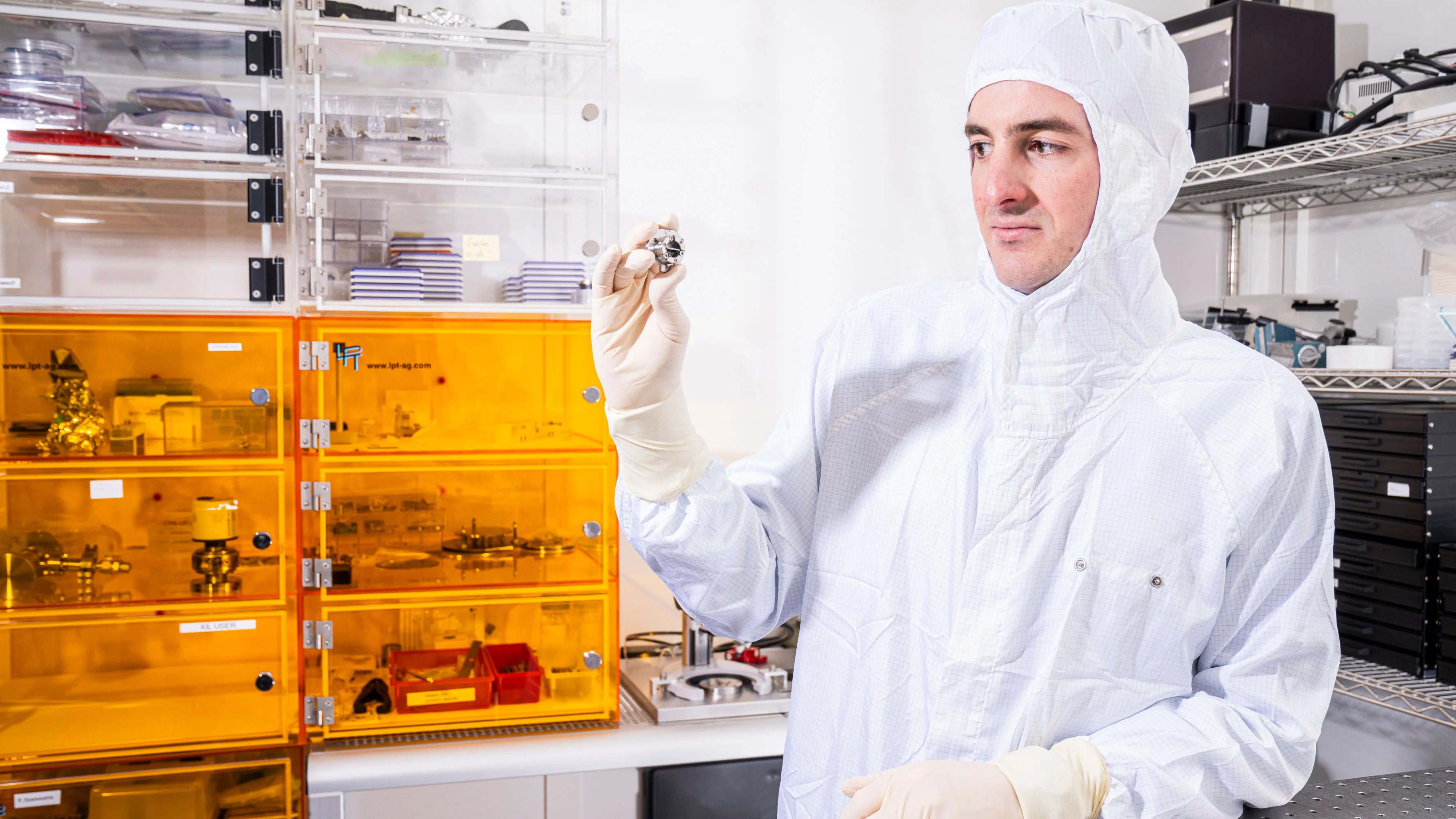
Researchers at the Paul Scherrer Institute PSI have been improving the resolution of a process known as photolithography. They hope to use their technique to help advance the miniaturisation of computer chips.
Microchips are produced like the pictures on a cinema screen
As recently as 1970, there was only room for around 1000 transistors on a microchip. Today, an area barely larger than the tip of a finger can hold about 60 billion components. These components are manufactured using a process called photolithography: a thin slice of silicon, the wafer, is coated with a light-sensitive layer, the photoresist. It is then exposed to a pattern of light corresponding to the blueprint for the microchip, which alters the chemical properties of the photoresist, making it either soluble or insoluble to certain chemical solutions. Subsequent treatment removes the exposed (positive process) or unexposed (negative process) regions. In the end, conductive tracks are left behind on the wafer forming the desired wiring pattern.
The type of light used is crucial for miniaturisation and for making microchips more and more compact. The laws of physics dictate that the smaller the wavelength of the light used, the more closely the structures in the image can be packed. For a long time, the industry used deep ultraviolet light (DUV). This laser light has a wavelength of 193 nanometres. By comparison, the range of blue light visible to the human eye ends around 400 nanometres.
Since 2019, manufacturers have been using “extreme ultraviolet light” (EUV) with a wavelength of 13.5 nanometres in mass production, more than ten times shorter than before. This makes it possible to print even finer structures, down to ten nanometres and less. At PSI, researchers use radiation from the Swiss Light Source SLS for their investigations, tuned to 13.5 nanometres in accordance with the industry standard.
Photon-based lithography can achieve very high resolution
However, the PSI researchers extended conventional EUV lithography by exposing the sample indirectly rather than directly. In EUV mirror interference lithography (MIL), two mutually coherent beams are reflected onto the wafer by two identical mirrors. The beams then create an interference pattern whose period depends on both the angle of incidence and the wavelength of the light. The group was able to achieve resolutions, i.e. track separations, of five nanometres – in a single exposure. Viewed under an electron microscope, the conductive tracks were found to have high contrast and sharp edges. Kazazis notes, “Our results show that EUV lithography can produce extremely high resolutions, indicating that there are no fundamental limitations yet. This is really exciting since it extends the horizon of what we deem as possible and can also open up new avenues for research in the field of EUV lithography and photoresist materials.”
A new EUVL tool from the end of 2025
At the moment, this approach is not interesting for industrial chip production, because it is very slow compared to industrial standards and can produce only simple and periodic structures rather than a chip design. However, it offers a method for the early development of photoresists needed for future chip production with a resolution that is not possible in the industry. The team plans to continue their research using a new EUV tool at the SLS, expected by the end of 2025. The new tool coupled with the SLS 2.0, which is currently going through an upgrade, will provide much enhanced performance and capabilities.
Contact
Original publication
-
Giannopoulos I, Mochi I, Vockenhuber M, Ekinci Y, Kazazis D
Extreme ultraviolet lithography reaches 5 nm resolution
Nanoscale. 2024; 16(33): 15533-15543. https://doi.org/10.1039/d4nr01332h
DORA PSI
Further information

About PSI
The Paul Scherrer Institute PSI develops, builds and operates large, complex research facilities and makes them available to the national and international research community. The institute's own key research priorities are in the fields of future technologies, energy and climate, health innovation and fundamentals of nature. PSI is committed to the training of future generations. Therefore about one quarter of our staff are post-docs, post-graduates or apprentices. Altogether PSI employs 2300 people, thus being the largest research institute in Switzerland. The annual budget amounts to approximately CHF 460 million. PSI is part of the ETH Domain, with the other members being the two Swiss Federal Institutes of Technology, ETH Zurich and EPFL Lausanne, as well as Eawag (Swiss Federal Institute of Aquatic Science and Technology), Empa (Swiss Federal Laboratories for Materials Science and Technology) and WSL (Swiss Federal Institute for Forest, Snow and Landscape Research). (Last updated in June 2024)