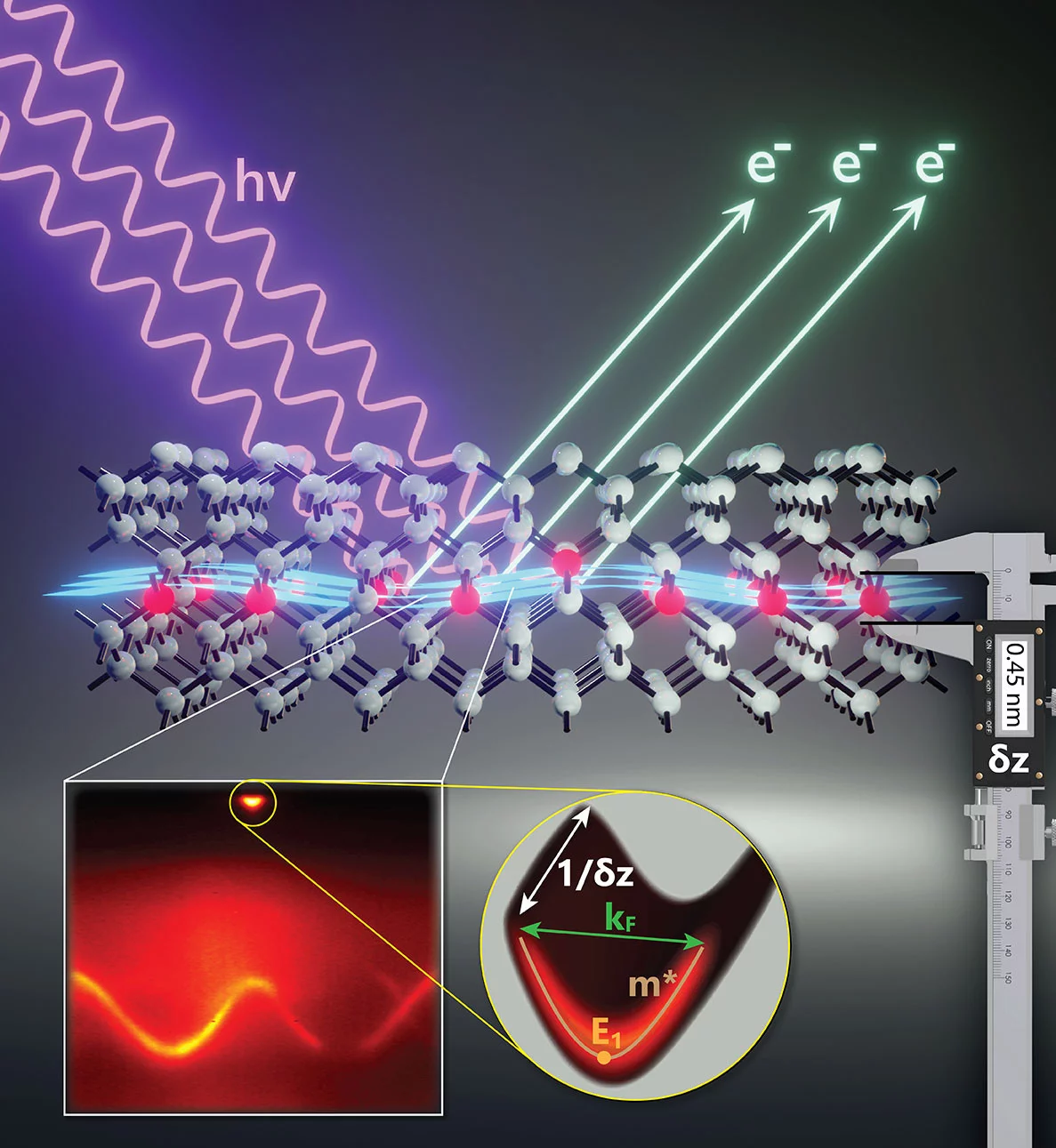
Soft X-rays at the Swiss Light Source SLS enable scientists to visualise non-invasively the electronic properties of ultra-thin dopant layers buried within semiconductor wafers. The ability to access this previously hidden information will give a boost to the design and development of quantum-electronic devices.
In the advancing world of semiconductor technologies and quantum computing, scientists are now able to engineer devices at the atomic scale. However, directly imaging the quantum waves in these buried, ultra-thin systems has proven to be a formidable challenge. Until now, doing so has involved invasive methods that ultimately destroy the system under investigation.
But imagine if we could illuminate the invisible and see the electrons within a silicon nanostructure without the invasive alteration of the host wafer itself. A team of researchers led by Dr Procopios Constantinou from the Paul Scherrer Institute (PSI) and Associate Professor Steven Schofield from University College London (UCL) have done just that. Their research, published in Advanced Science, has opened a new window into the unseen world of atomic-scale devices.
Two-dimensional electron liquids: the building blocks of quantum computers
Advances in solid-state fabrication have enabled the precise placement of single dopant atoms within a silicon host. These dopant atoms, when packed into high-density atomically thin planes, create two-dimensional electron liquids (2DELs) in the silicon host that are the thinnest of their kind and offer novel functionalities. Such two-dimensional dopant layers, also known as δ-layers (“delta” layers) in semiconductors, provide high-mobility 2DELs that are needed as building blocks for future quantum computers and play a crucial role in next-generation transistor technologies. Traditionally, key parameters of 2DELs (such as carrier densities, effective masses, and confinement thicknesses defining the extent of the electron waves perpendicular to the δ-layer) have been extracted from electrical resistance measurements, which require the destructive fabrication of the sample into a device geometry, as well as theory linking the transport of electrons to their fundamental wave-like properties. In their new work, the team used soft X-rays to measure the properties of these buried electron liquids directly on as-grown wafers.
Soft X-ray ARPES reveals thinnest ever 2D electron liquids in silicon
The researchers used a method pioneered at the ADRESS beamline of the SLS at PSI, known as angle-resolved photoelectron spectroscopy using soft X-rays – or SX-ARPES for short. Their measurements, reported in Advanced Science, revealed that dopant layers made from arsenic host the thinnest technological 2D electron liquids ever fabricated in silicon, with an electronic thickness of 0.45 ± 0.04 nm, comparable to the silicon lattice parameter (0.54 nm). The samples were fabricated in London and measured in Switzerland after exposure to ambient conditions. This highlights the ability to measure δ-layers through the resulting surface oxide, showcasing the technological compatibility of the method and the remarkable stability of these ultra-thin, high-density δ-layer systems. Given that the dopant phosphorus has dominated the field of atomic-scale devices in silicon for over two decades, this finding could have significant implications for the design and performance of future quantum-electronic devices.
The research provides direct images of the electronic motion in δ-layers in silicon and will lead to new tools to characterize semiconductor nanostructures and devices. With next-generation light sources and new optics, both to be installed as part of the SLS 2.0 upgrade at PSI, SX-ARPES with time resolution and sub-micron precision (SX-nanoARPES) will be possible, enabling the imaging of the electronic waves in semiconductor devices as they are switched. This will complement X-ray inspection of integrated circuit morphology and chemical composition, both also pioneered at PSI.
Now published in Advanced Science, this research represents a significant step forward which opens exciting new possibilities for the future of semiconductor technologies and quantum computing.
Text: PSI/UCL, Schofield, Constantinou and Aeppli
© PSI provides image and/or video material free of charge for media coverage of the content of the above text. Use of this material for other purposes is not permitted. This also includes the transfer of the image and video material into databases as well as sale by third parties.
Contact
Dr Procopios Constantinou
Photon Science Division
Paul Scherrer Institut, 5232 Villigen PSI, Switzerland
Email: procopios.constantinou@psi.ch
Assoc. Prof. Dr. Steven R. Schofield
London Centre for Nanotechnology
University College London, London, WC1H 0AH, UK
Email: s.schofield@ucl.ac.uk
Prof. Dr. Gabriel Aeppli
Photon Science Division
Paul Scherrer Institut, 5232 Villigen PSI, Switzerland
Department of Physics & Quantum Center
Eidgenössische Technische Hochschule Zürich, 8093 Zürich, Switzerland
Institute of Physics
Ecole Polytechnique Fédérale de Lausanne, 1015 Lausanne, Switzerland
Email: aepplig@ethz.ch
Original Publication
Momentum-Space Imaging of Ultra-Thin Electron Liquids in δ-Doped Silicon
Procopios Constantinou, Taylor J. Z. Stock, Eleanor Crane, Alexander Kölker, Marcel van Loon, Juerong Li, Sarah Fearn, Henric Bornemann, Nicolò D'Anna, Andrew J. Fisher, Vladimir N. Strocov, Gabriel Aeppli, Neil J. Curson, Steven R. Schofield
Advanced Science, 2023, 2302101
DOI: https://doi.org/10.1002/advs.202302101

