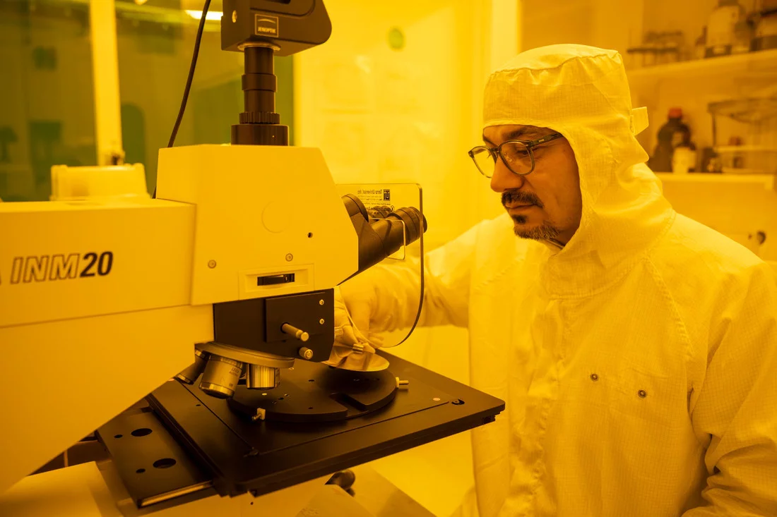
The Paul Scherrer Institute PSI and the Finnish company PiBond are collaborating to commercially leverage advanced semiconductor products manufactured using EUV lithography. Lithography is crucial for semiconductor technology, playing a key role in faster and more energy-efficient semiconductor chips, particularly for artificial intelligence. PiBond leads in the development of lithographic materials and collaborates with PSI to address these challenges and drive forward new photoresist technologies. PiBond has licensed cutting-edge lithography technologies from PSI with the aim of further developing them. The strategic collaboration aims to promote innovations in semiconductor technology and provide solutions for industry needs. PiBond has established a subsidiary in Switzerland, based at the Switzerland Innovation Park Innovaare, in close proximity to PSI. The partnership between PSI and PiBond enables significant progress and offers new opportunities for the future. This collaboration is valued and promising from both sides, demonstrating a commitment to innovation and technological advancement.

