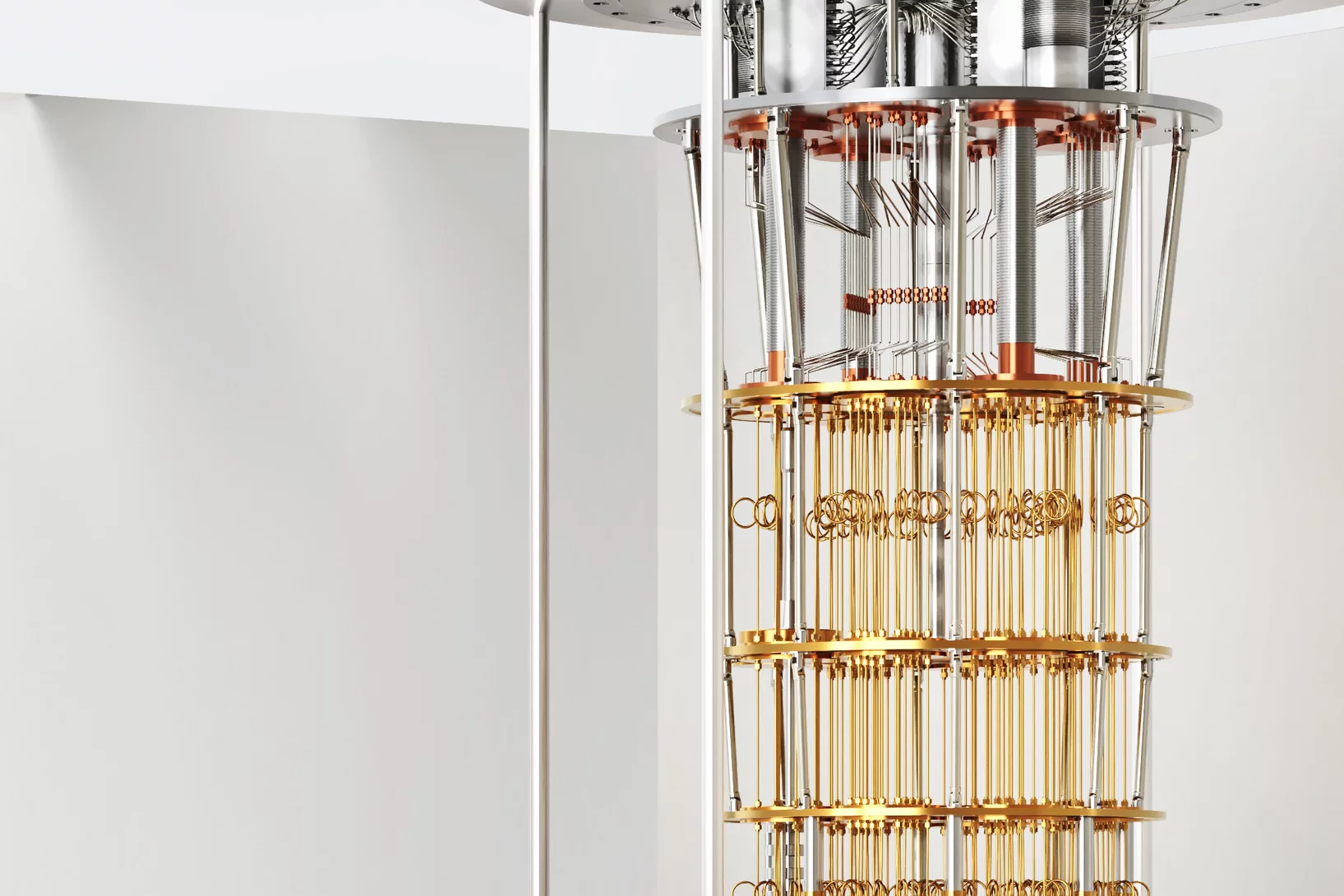
Unique quantum simulator opens door to new research
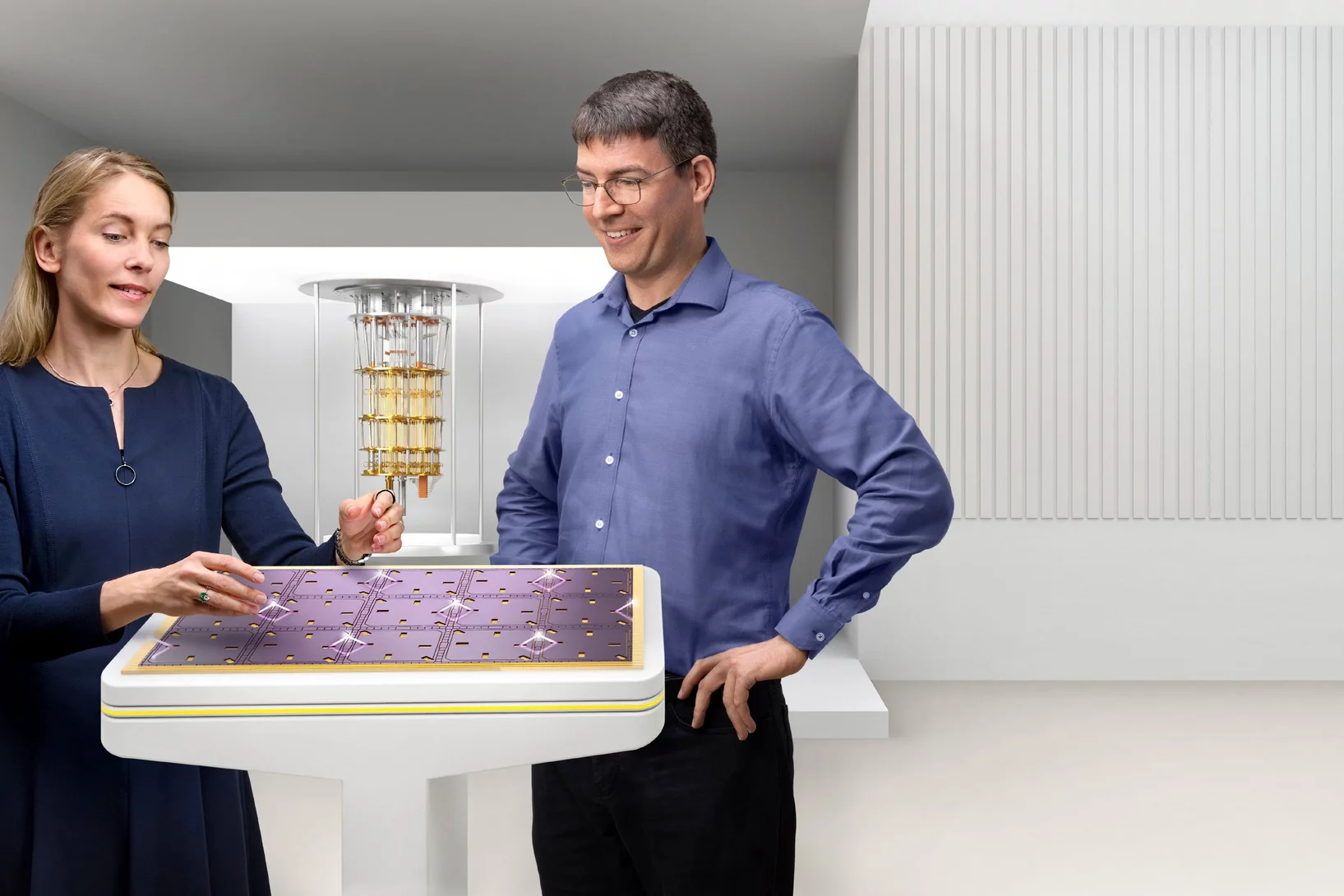
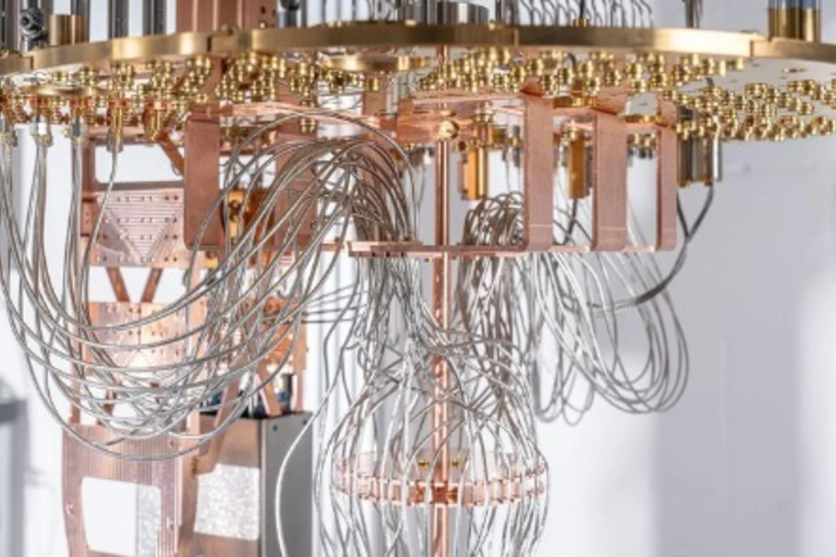
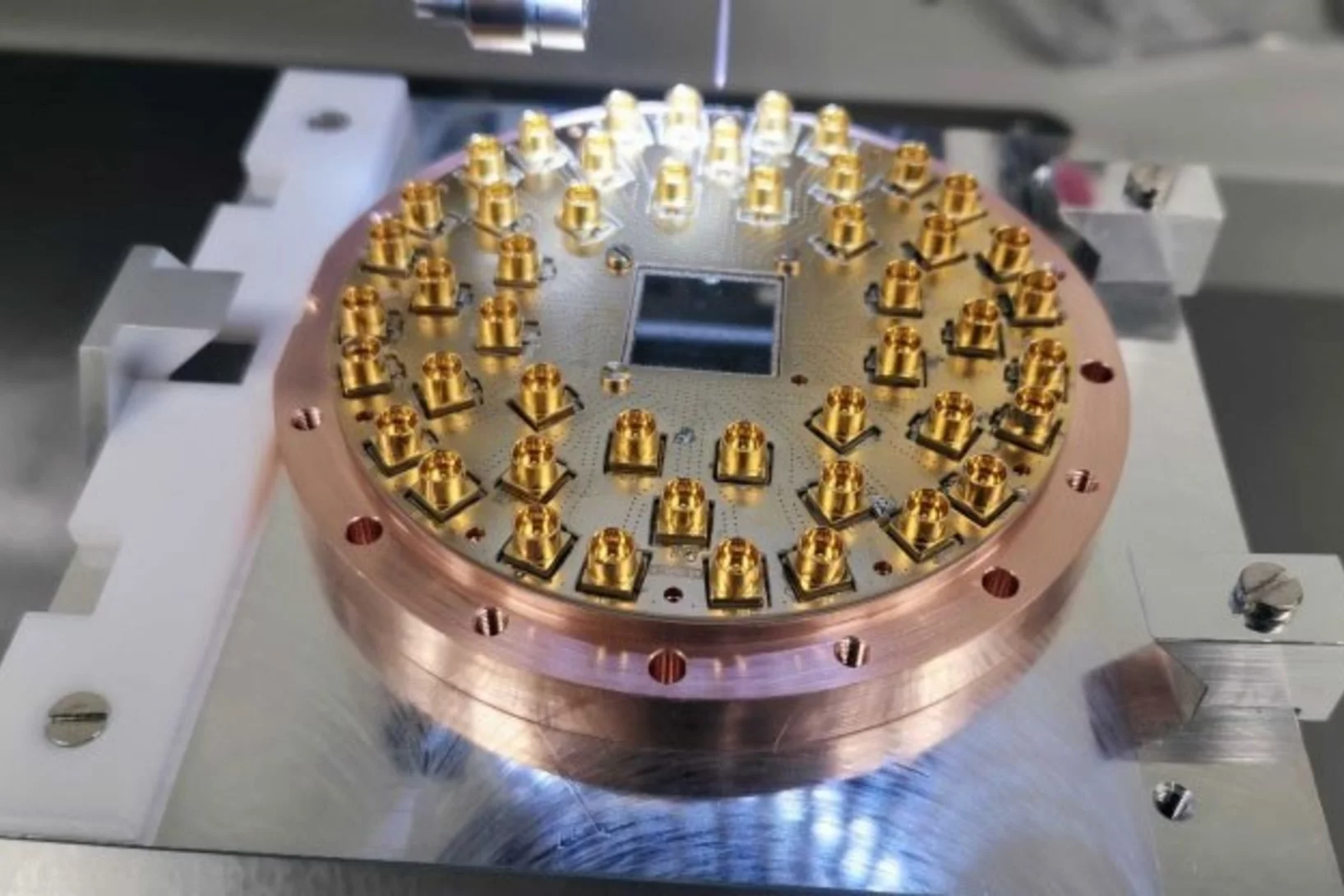
PSI physicists have teamed up with Google to build a new type of digital-analogue quantum simulator.
Congratulations to Lis Alaball for successful PhD thesis defence
Congratulations to Lis Alaball for successful defense of her PhD project titled "Quantifying bacterial responses to antibiotics at the single-cell level".
Lis developed new microfluidic designs that together with microscopy and image analysis tools, allow the tracking of single bacterial cells over the time course of antibiotic treatments. Her reasearch project was supported by SNI PhD School program (P1805).
First Light in IPN's New Nanophotonic Setup
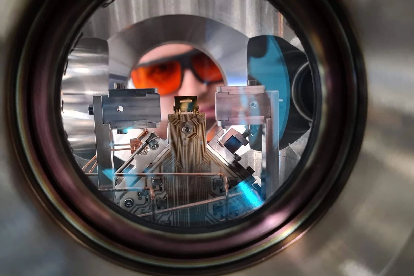
The Integrated Photonics & Nanoelectronics Team made a fantastic job in the last weeks rebuilding their optical setup at Park Innovaare. Today marked a milestone in the successful restart of measurements, as all instruments of the main micro-photoluminescence setup were tested and the first calibartion taken. The group looks forward to installing all other remaining components and going through a meticulous alignment routine.
Sustainable Group-IV Active Photonics Research Sinergia Project granted
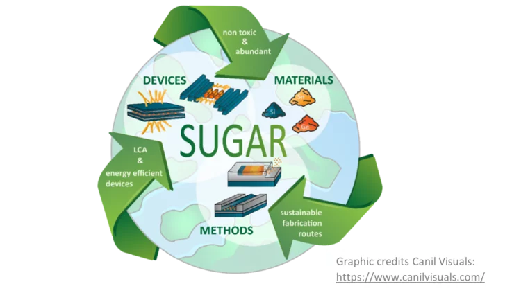
We are excited to announce that our joint Sinergia Project: Sustainable Group-IV Active Photonics Research (SUGAR) has been approved for funding by the SNSF and will start in the spring of 2024. SUGAR is an interdisciplinary project that aims to develop a more sustainable photonics platform, based on group IV elements (Si, Ge, Sn). The proposal emphasizes sustainability throughout the entire device life-cycle, incorporating life cycle assessment (LCA) from extraction to end-of-life.
Park Innovaare Cleanroom Name is: PICO
We are happy to announce that the new Cleanroom Name in the Park Innovaare will be PICO = Park Innovaare Cleanroom for Optics and innovation.
Next Step – we will work on a Logo (ideas welcome), together with PiA.
The winner of the naming contest: Helmut Schift
Two projects launched to connect error-corrected qubits
Researchers at ETH Zurich and PSI are participating in two quantum computing projects that are being financed by the US research funding agency IARPA.
Using quantum computers already today
Analogue quantum computers make ultrafast chemical reactions observable.
Open Quantum Institute launch
Dr. Cornelius Hempel, head of the Ion Trap Quantum Computation group at LNQ’s ETHZ-PSI Quantum Computing Hub, spoke to SRF to explain how quantum computers work and how future versions of these devices can be used to solve some of the big problems of our time.
Der Wettlauf um den Quantencomputer
Der Wettlauf um den Quantencomputer
Forschung online erleben
Sehen Sie hier die Aufzeichnung des Live-Video-Rundgangs vom 23. August 2023
LNQ-BBQ
LNQ-BBQ on 27.06.2023
Swiss PIC to support Swiss photonics industry
The technology transfer centre Swiss PIC will be located in the Park Innovaare.
Nanotechnology group is welcoming Kevin Hofhuis
Starting in Novemeber 2022, Dr. Kevin Anthony Hofhuis joined the Nanotechnology group as an E-beam Lithography Scientist.
Welcome to the cleanroom team, Kevin!
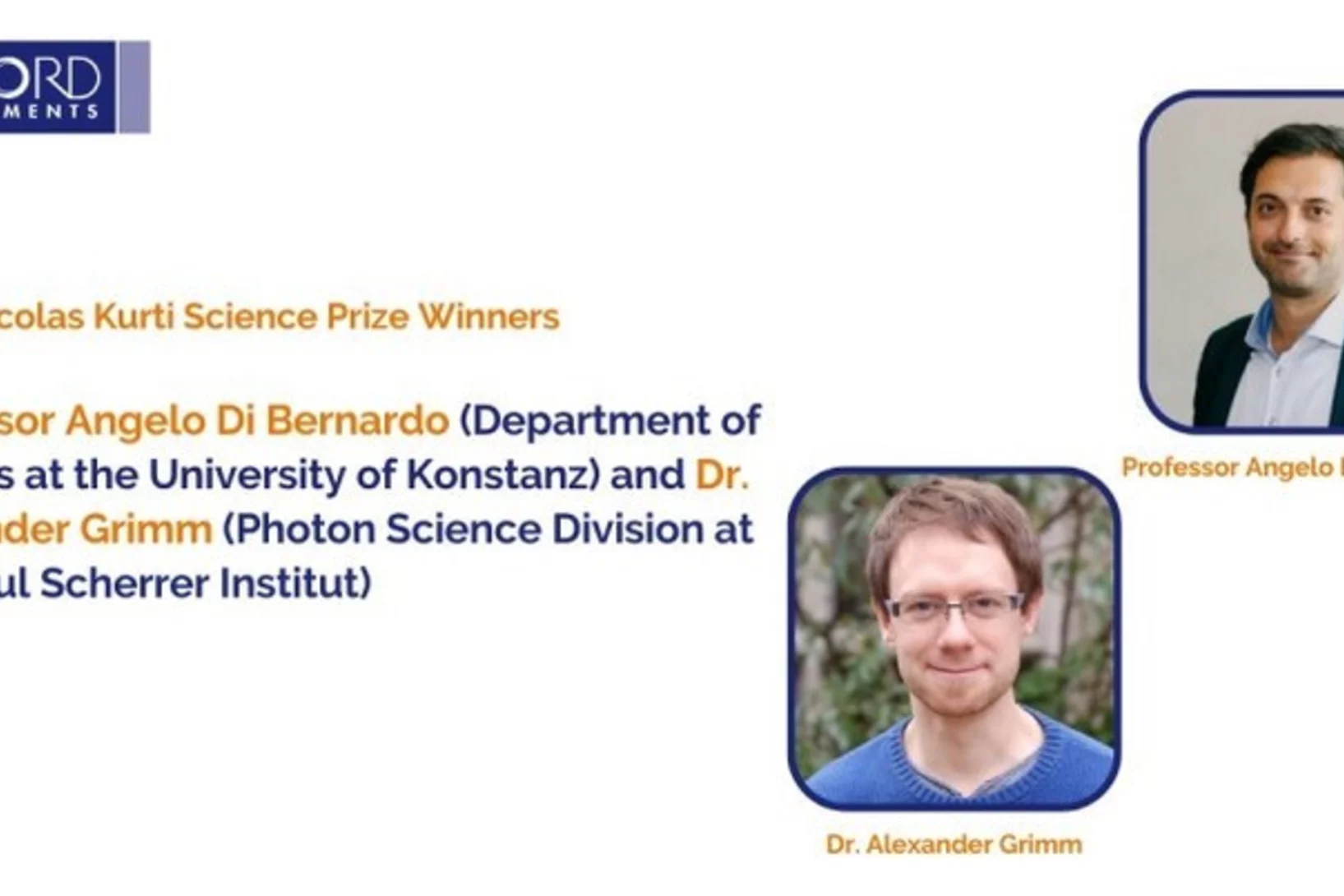
Alexander Grimm wins 2022 Nicholas Kurti prize
We are happy to announce that Alex has been awarded the 2022 Nicholas Kurti Science prize. The prize recognises his work on non-linear effects in Josephson junctions for quantum information processing.
Capturing control errors in quantum annealing
The real-world application of this type of quantum computing gets one step closer with a new method to capture errors while qubits are talking to each other.
Solving the unsolvable
PSI and ETH Zurich have founded the Quantum Computing Hub, where top researchers work together on concepts for quantum computers.
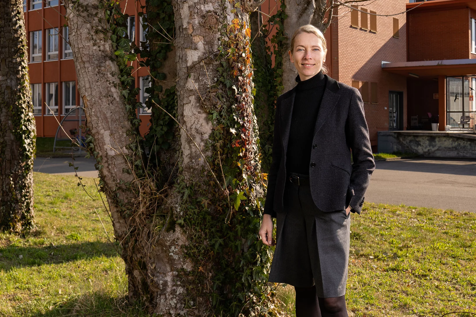
“If you’re in a certain position, you should step forward”
Kirsten Moselund heads the new Laboratory for Nano and Quantum Technologies. In this interview she discusses quantum research at PSI and how nanophotonics can assist with this.
LNQ Kick-off
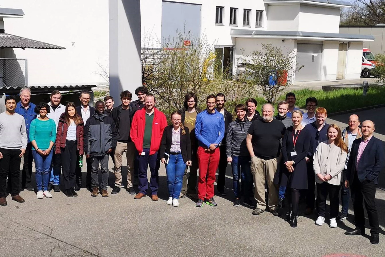
On April 11th, we had the opportunity to celebrate the kick-off meeting of the new Laboratory of Nano and Quantum Technologies (LNQ), and many had the chance to meet their new colleagues for the first time. Presently, our lab joins together two cleanroom-technology focused groups, Nanotechnology led by Dr. Vitaliy Guzenko and Advanced Nanomanufacturing by Dr. Helmut Schift, respectively, with groups focusing on three different technology platforms in quantum computing. These are Ion trap Quantum Computing led by Dr. Cornelius Hempel, Superconducting Quantum Circuits that is an extension of Prof. Andreas Wallraff's activities at ETHZ, and Neutral Atoms Quantum Engineering, which will be led by Prof. Wenchao Xu joining in August.
Superconducting qubit first success at Quantum Computing Hub
Andreas Wallraff talks about moving in, refrigerators and measuring the first superconducting qubit at the ETHZ-PSI Quantum Computing hub.
New Confocal Microscope Keyence VK-X3100
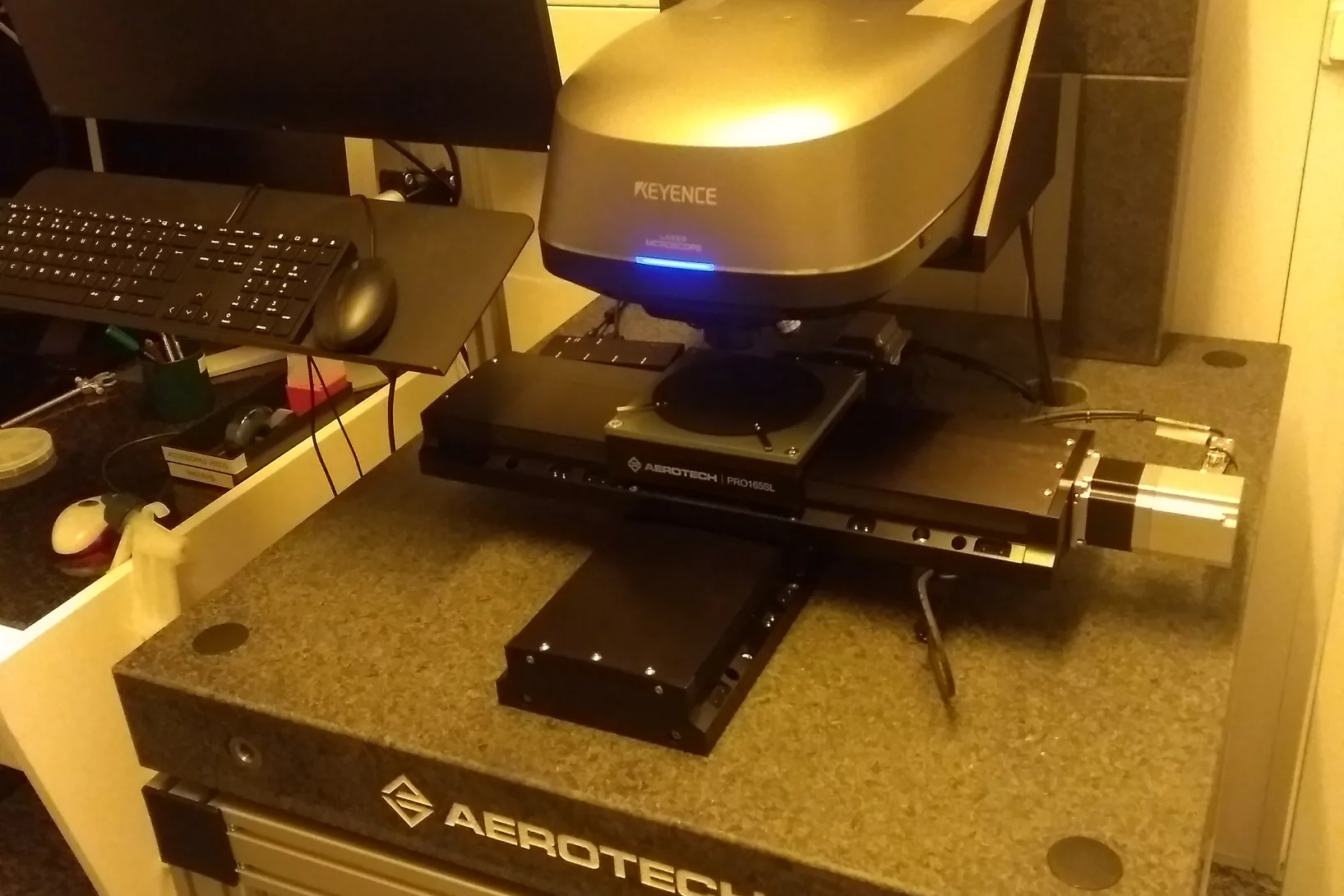
Keyence VK-X3100 is a non-contact 3D surface profiler. It enables capturing images and performing the profile, roughness and film thickness analysis. The measurement head is equipped with semiconductor laser with the wave length of 404 nm and white LED. To reach the best performance, it uses laser confocal scanning, focus variation, adn while light interferometry measurement methods. The motorized sample stage allows for automatic inspection of up to 200mm wafers.
Installation of SPTS Rapier Deep Reactive Ion Etcher
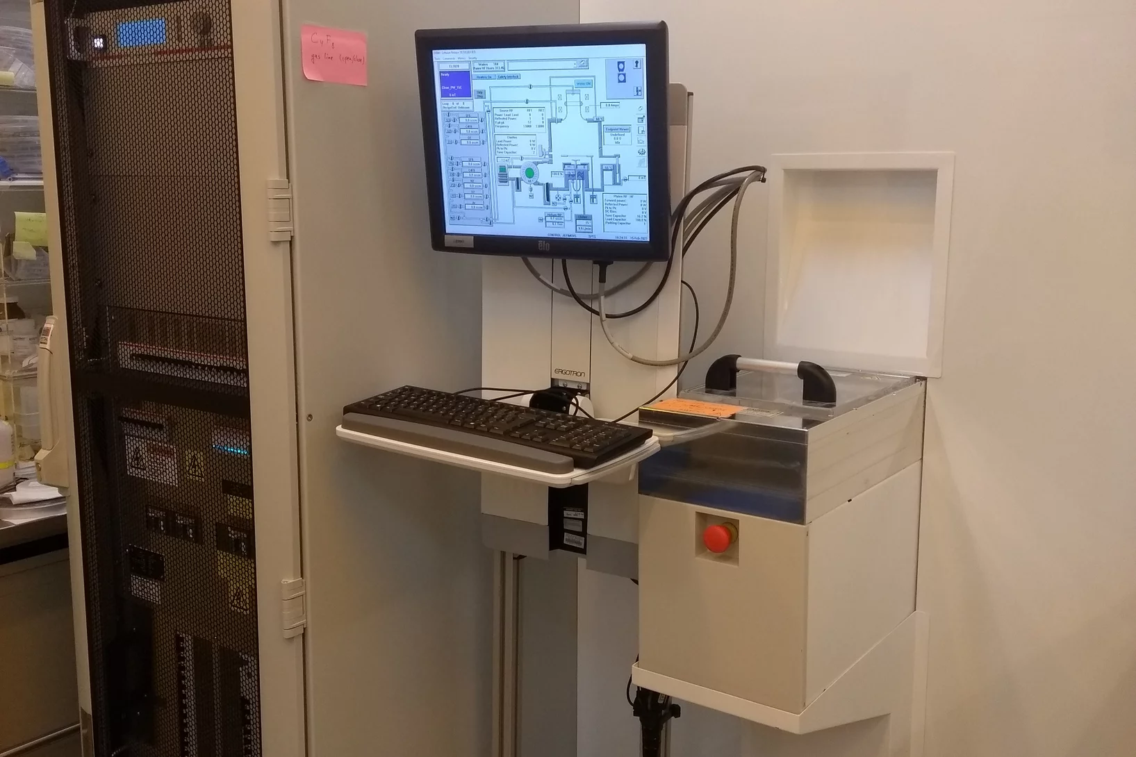
SPTS Rapier system for Si deep reactive ion etching (DRIE) is released for user operation. The system is acquired by PSI as a part of SNF R’Equip project “Advanced Si DRIE tool for highly uniform ultra-deep structuring (SiDRY)”. This versatile tool is equipped with pulsed bias option and sensitive ClaritasTM optical end point detection system. Electrostatic clamping and wafer edge protection systems are both available for three wafer diameters – 100 mm, 150 mm, and 200 mm.
