

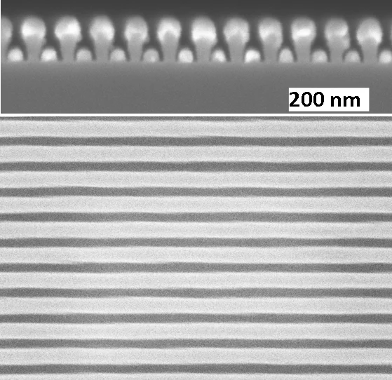
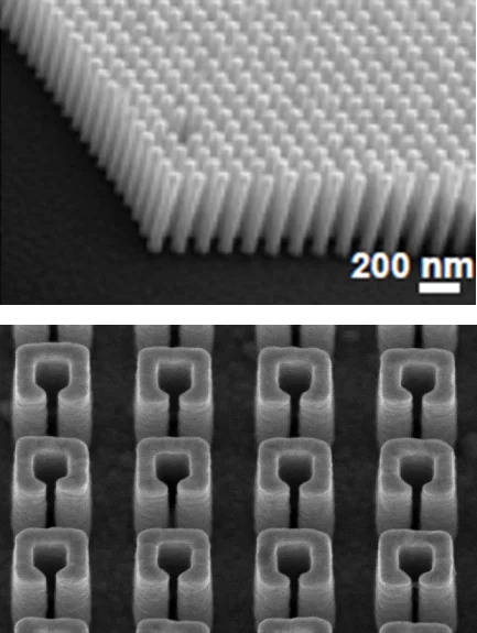
Metallic nanostructures smaller than wavelength of interacting radiation have interesting far-field and near-field optical properties. For instance, the electromagnetic fields near such structures (near fields) are significantly amplified. This phenomenon is important for applications such as near-field microscopy, biosensing, surface enhanced Raman spectroscopy and nano-antennae. Also far-field properties of such structures are substantially different and can be tailored resulting in exciting phenomena such as extraordinary transmission through subwavelength hole arrays, negative refractive index, and strong birefringence. Our aim is to design novel nanomaterials for potential applications in nanophotonics, nanoplasmonics, biosensing and optical devices. The fabrication methods involve e-beam lithography and extreme ultraviolet interference lithography.
Selected Publications
Distributing the optical near-field for efficient field-enhancements in nanostructures,
V. K. Valev, B. De Clercq, C. G. Biris, X. Zheng, S. Vandendriessche, M. Hojeij, D. Denkova, Y. Jeyaram, N. C. Panoiu, Y. Ekinci, A. V. Silhanek, V. Volskiy, G. A. E. Vandenbosch, M. Ameloot, V. V. Moshchalkov, and T. Verbiest,
Adv. Mater. (2012).
Deep-ultraviolet surface-enhanced resonance Raman scattering of adenine on aluminum nanoparticle arrays,
S. K. Jha, Z. Ahmed, M. Agio, Y. Ekinci, and J. F. Löffler,
J. Am. Chem. Soc. 134, 1966 (2012).
High Aspect Ratio Plasmonic Nanostructures for Sensing Applications,
B. Päivänranta, H. Merbold, R. Giannini, L. Buechi, S. Gorelick, C. David, J. F. Löffler, T. Feurer, Y. Ekinci,
ACS Nano 5, 6374 (2011).
Nanofluidics
Trapping, sorting and manipulation of nanoparticles in solution are of great interest for applications in soft condensed matter, biology, and medicine. We develop methods and devices based on nanofluidics for reliable, high-throughput and contact-free trapping, manipulation of nanoparticles and nano-objects.
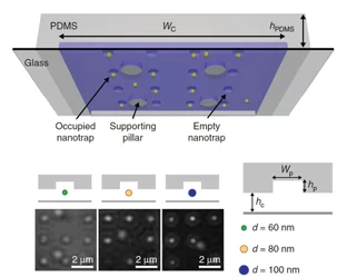
pillars. The nanofluidic channels had a width of several micrometers and the height is a few hundred nanometers and nanopockets. Below show the optical images of trapped nanoparticles.
Selected Publications
Soft electrostatic trapping in nanofluidics
M. A. Gerspach, N. Mojarad, D. Sharma, T. Pfohl, and Y. Ekinci
Nature Microsystems & Nanoengineering 3, 17051 (2017)
Nanofluidic lab-on-a-chip trapping devices for screening electrostatics in concentration gradients
M. A. Gerspach, N. Mojarad, D. Sharma, T. Pfohl, and Y. Ekinci
Microelectronic Eng. 175, 17 (2017)
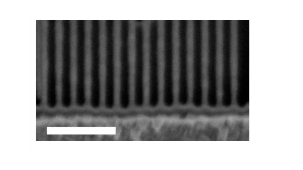
Nanowires
Selected Publications
Strain and thermal conductivity in ultra-thin suspended silicon nanowires
D. Fan, H. Sigg, R. Spolenak, and Y. Ekinci
Physical Review B 96, 115307 (2017)
Nanocatalysis
Selected Publications
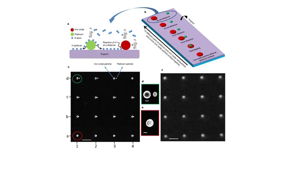
Catalyst support effects on hydrogen spillover
W. Karim, C. Spreafico, A. Kleibert, J. Gobrecht, J. VandeVondele, Y. Ekinci, and J. A. van Bokhoven
Nature 541, 68 (2017)
Size-dependent redox behavior of iron observed by in-situ single nanoparticle spectro-microscopy on well-defined model systems
W. Karim, A. Kleibert, U. Hartfelder, A. Balan, J. Gobrecht, J. A. van Bokhoven, and Y. Ekinci
Scientific Reports 6, 18818 (2016)