

- Development of technology for lensless imaging for advanced semiconductor manufacturing
- A state-of-the-art prototype for EUV actinic mask inspection
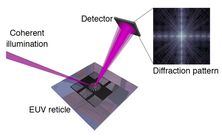
Metrology branch of XIL-II beamline provides spatially coherent illumination and monochromatic beam of up to λ/Δλ=1600 in the range of 10 nm to 16 nm wavelength. We develop photomask inspection technology with coherent scattering contrast and imaging with coherent diffractive imaging. The advantages are being lensless and providing both amplitude and phase information of the sample.
EUV mask inspection
EUV photomasks are used in semiconductor manufacturing as a master to transfer the circuit design on silicon. They consist of a 120×120×6 mm glass substrate with a Mo/Si multilayer coating for maximum reflectance at 6° and λ =13.5 nm. They have to be inspected to detect and remove defects that may disrupt the design and hamper the functionality of the semiconductor device. Detecting a defect smaller than 50 nm on a photomask with a precision of a few nanometers is like finding a tennis ball on a surface as large as Switzerland.
Selected Publications
RESCAN: an actinic lensless microscope for defect inspection of EUV reticles
I. Mochi, P. Helfenstein, I. Mohacsi, R. Rajeev, D. Kazazis, S. Yoshitake, and Y. Ekinci
J. Micro/Nanolith. MEMS MOEMS 16(4), 041003 (2017)
doi: 10.1117/1.JMM.16.4.041003
Scanning coherent diffractive imaging methods for actinic EUV mask metrology
P. Helfenstein, I. Mohacsi, R. Rajendran, and Y. Ekinci
J. Micro/Nanolith. MEMS MOEMS 15(3), 034006 (2016)
doi: 10.1117/1.JMM.15.3.034006