

Since 2005 LMN is operating a Zeiss Supra VP55 high resolution field emission scanning electron microscope.
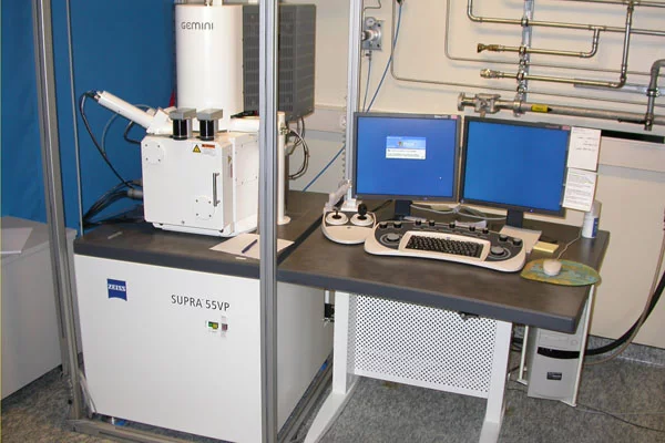
Zeiss Supra VP55 SEM operated by the Lab for Micro and Nanotechnology at PSI
Details of the Instrument
- Column based on GEMINI principle
- Installed in 2005
- Cathode: thermal field emission tip (Schottky-emitter ZrO/W)
Detector possibilities
- In Lens detector for secondary electrons gives highest spatial resolution with specification of 1nm at an acceleration voltage of 15kV (Au on C- sample)
- Everhardt Thornley detector for secondary electrons
- Backscattered electron detector Centaurus especially useful for enhanced material contrast
- Variable Pressure detector for imaging e.g. electrically nonconductive, degassing materials without the need for metal coating. This works by charge compensation (positively ionised gas molecules stabilise local charging). Spatial resolution: approx. 3nm @ 15kV