

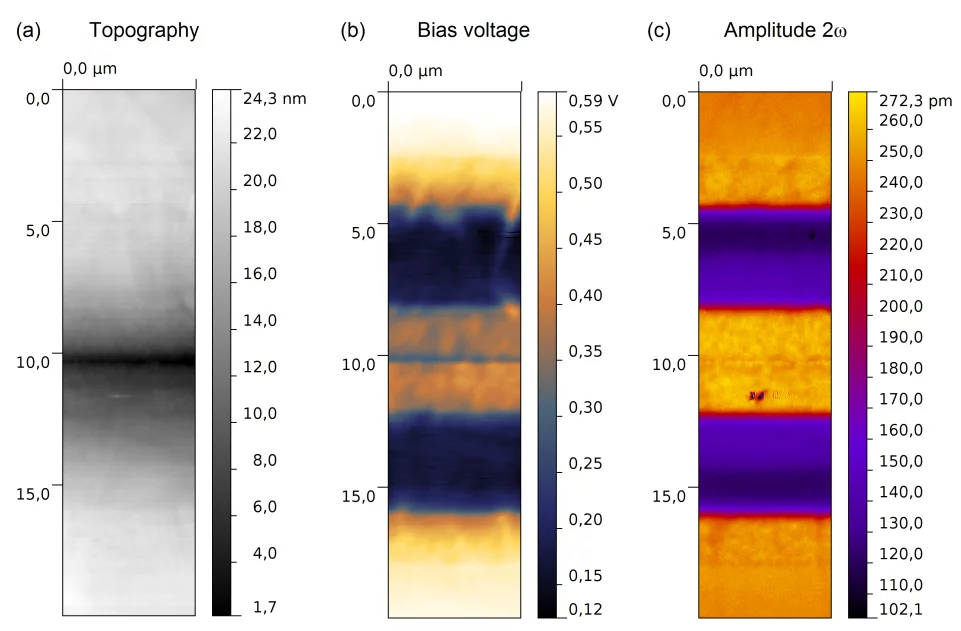
For power semiconductor devices the two main figures of merit are (i) a high blocking voltage capability, which minimizes the re‐ verse current in the OFF‐state and (ii) a low ON‐state resistance when the device is operated under forward conditions. The mate‐ rial properties of silicon carbide are expected to be superior to sili‐ con because of their higher critical electric field and higher thermal conductivity. This properties can be integrated into devices like Schottky diodes, MOS capacitors and planar MOSFETs. Thereby higher switching speeds can be achieved at lower power dissipa‐ tion. A significant challenge and current limitation in performances of active devices is due to the low channel mobilities inside the in‐ version channel at the 4H‐SiC/insulator interface and the increas‐ ing junction‐FET resistance causing the downscaling of these de‐ vices. Various interface passivation treatments therefore have been tested which resulted in a slight mobility improvement of current devices. However the ob‐ tained mobilities are still far below the theoretical bulk value and the physical origin of the mobility enhancing mechanism still remains unclear.
Current research activities:
- Atomic‐Scale Analysis of SiC‐Oxide Interface for Improved High‐Power MOSFETs [1]
- Wide Band Gap Power Semiconductors Improved by Nanoscale Probe Analytics [2]
- Physical Studies of SiC Nano‐Trench‐MOSFETs [3]
[1] Evidence for carbon clusters present near thermal gate oxides affecting the electronic band structure in SiC-MOSFET.
D. Dutta et al.
Editor’s Pick in Appl. Phys. Lett. 115, 101601 (2019);
[2] Improving the Design of the Shield for the Electric Field in SiC-Based Schottky-Rectifiers and Ion-Implantation Cascades by SPM Dopant-Imaging.
H. Rossmann et al.
Microelectronic Engineering 148 (2015) 1–4
[3] Device Simulations on Novel High Channel Mobility 4H-SiC Trench MOSFETs and Their Fabrication Processes
H. R. Rossmann, A. Bubendorf, F. Zanella, N. Marjanović, et al.
Microelectron. Eng. 145, 166 (2015)