

- EUV-IL is a powerful and cost-effective tool for resist evaluation for future technology nodes in semiconductor manufacturing
- Providing nanostructures for various projects and applications in nanoscience with high resolution and large area
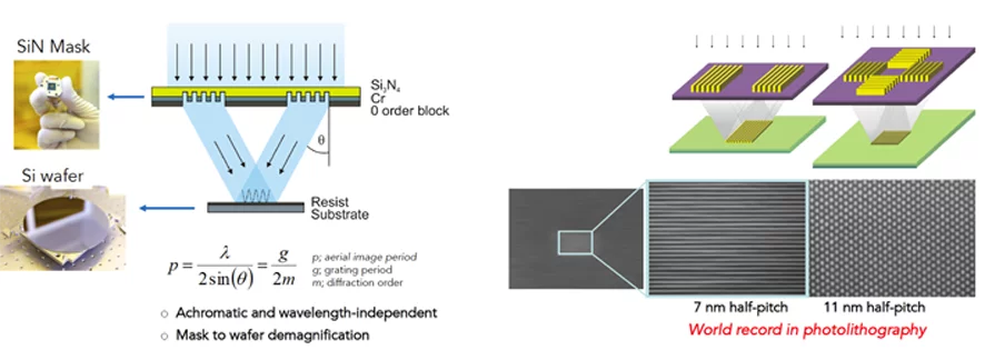
- Proven the world record resolution capabilities by showing a large-area patterns down to 6 nm half-pitch
Progress in nanotechnology is essential for producing faster computers and high-density data storage. This progress is fueled by the downscaling of integrated circuit (IC) technology, which was predicted decades ago by Gordon Moore. Currently high-volume semiconductor manufacturing uses the optical double patterning methods and immersion lithography at the wavelength of 193 nm to reach the 22 nm node but these techniques may reach their limits because of fundamental limitations. Therefore, particular interest is channeled towards extreme ultraviolet (EUV) lithography at the wavelength of 13.5 nm, whereas its cost-effective introduction requires further development of resists capable of printing dense patterns down to this resolution in addition to other challenges such as development of powerful light sources.
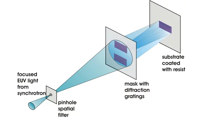
In parallel with the projection optical systems developed for industrial applications, EUV interference lithography (EUV-IL) is a powerful tools for both scientific and industrial research. Our industrial research focuses mainly of developing novel high-resolution resists. In addition, the advantage of being a parallel fabrication process with both high resolution and throughput makes EUV-IL attractive for academic research.
For image forming EUV-IL requires spatially coherent illumination and transmission diffraction gratings. EUV-IL tool at PSI is the world-leading tool reaching a resolution down to 6 nm half-pitch.
High-resolution Patterning
- Stable light source: Synchrotron undulator
- Spatial coherent illumination
- Variable wavelength: 16 nm to 3 nm
- Diffractive transmission gratings on SiN membranes
- Interference pattern printed in resist
- Stable interferometer
- No depth of focus
- Excellent reproducibility
- On-site processing in cleanroom
- Well-defined aerial image
- High resolution
- High throughput
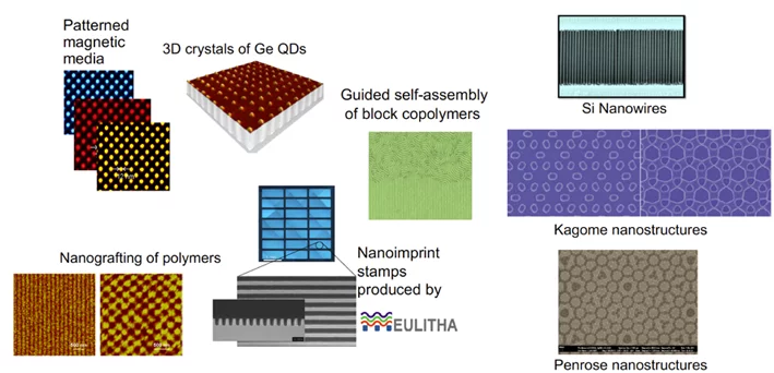
Applications:
- EUV resist development
- Nanoimprint stamps
- Fluidic confinement structures
- Plasmonics and Metamaterials
- Polymer grafting
- Biomaterials
- Catalysis
- Templated assembly
- Cell growth templates
- Nanomagnetism
- Fresnel Zone Plates
- etc.
Selected Publications
Nanolithography using Bessel beams of extreme ultraviolet wavelength
D. Fan, L. Wang, and Y. Ekinci
Scientific Reports 6, 31301 (2016)
Photolithography reaches 6 nm half-pitch using extreme ultraviolet light
D. Fan and Y. Ekinci
J. Micro/Nanolith. MEMS MOEMS 15(3), 033505 (2016)
High-resolution and large-area nanoparticle arrays using EUV interference lithography
W. Karim, S. A. Tschupp, M. Oezaslan, T. Schmidt, J. Gobrecht, J. van Bokhoven, and Y. Ekinci
Nanoscale 7, 7386-7393 (2015)
Fabrication of quasiperiodic nanostructures with EUV interference lithography,
A. Langner, B. Päivänranta, B. Terhalle, and Y. Ekinci,
Nanotechnology 23, 105303 (2012).
Sub-10 nm patterning using EUV interference lithography,
B. Päivänranta, A. Langner, E. Kirk, C. David, and Y. Ekinci,
Nanotechnology 22, 375302 (2011).