

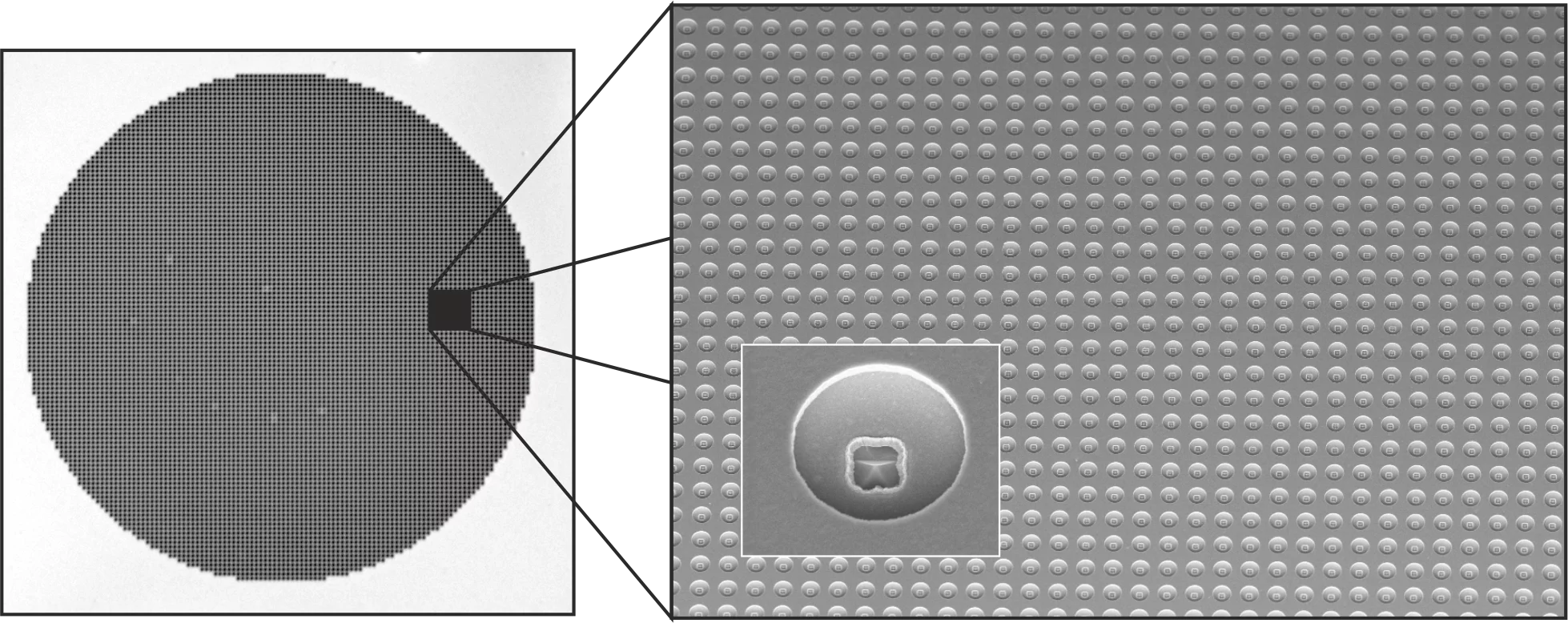
Double-gate field emitter array equipped with a collimation gate electrode for the individual emitters in addition to an electron extraction gate electrode can reduce the rms transverse electron veloecy of the field emission beamlet and the emittance of the FEA beam. We have shown recently that an order of magnitude reduction of the rms transverse electron velocity can be achieved with our structure with minimal reduction of the emission current [1,2,3,4]. Further effort to match the cathode spec [5,6] for the SwissFEL X-ray free electron laser [7] is under way.
Although high current FEAs have been intensively studied to realize a compact vacuum electronic amplifier, such as traveling wave tubes (TWTs) [8,9,10], and working FEA-TWT in 5 GHz range with 100 W output have been already demonstrated [10], double-gate FEAs with low normalized emittance will be essential to fully take advantage of the high current density characteristic of FEAs, in particular for the compact THz amplifiers [11,12] and THz power modules (a the vacuum electronic amplifiers seeded by solid-state low-power oscillators) [e.g. 13]. These FEAs may also be applicable for the massively parallel electron beam lithography tools [e.g. 14].
References
[1] S. Tsujino, P. Helfenstein, E. Kirk, T. Vogel, C. Escher, and H.-W. Fink, Field-emission characteristics of molded molybdenum nanotip arrays with stacked collimation gate electrodes, IEEE Electron Device Letters, vol. 31, 1059 (2010).
[2] P. Helfenstein, E. Kirk, K. Jefimovs, T. Vogel, C. Escher, H.-W. Fink, and S. Tsujino, Highly collimated electron beams from double-gate field emitter arrays with large collimation gate apertures, Appl. Phys. Lett. 98, 061502 (2011).
[3] P. Helfenstein, K. Jefimovs, E. Kirk, C. Escher, H.-W. Fink, and S. Tsujino, Fabrication of metallic double-gate field emitter arrays and their electron beam collimation characteristics, J. Appl. Phys. 112, 093307 (2012).
[4] P. Helfenstein, V. A. Guzenko, H.-W. Fink, and S. Tsujino, Electron beam collimation with a 40 000 tip metallic double-gate field emitter array and in-situ control of nanotip sharpness distribution, J. Appl. Phys. 113, 043306 (2013).
[5] M. Dehler, A. Candel, E. Gjonaj, Full scale simulation of a field-emitter arrays based electron source for free-electron lasers, J. Vac. Sci. Tech. B 24,892-897 (2006).
[6] M. Dehler, Design and modeling of field emitter arrays for a high brilliance electron source, Proceedings of the 9th International Computational Accelerator Physics Conference (ICAP2006), (Chamonix, France, 2-6, Oct. 2006).
[7] B. Patterson, R. Abela, H.-H. Braun, U. Flechsig, R. Ganter, Y. Kim, E. Kirk, A. Oppelt, M. Pedrozzi, S. Reiche, L. Rivkin, Th. Schmidt, B. Schmidt, V. N. Strocov, S. Tsujino, and A. F. Wrulich, New J. Physics, 12, 035012 (2010).
[8] H. Makishima, S. Miyano, H. Imura, J. Matsuoka, H. Takemura, and A. Okamoto, Design and performance of traveling-wave tubes using field emitter array cathodes, Appl. Surf. Sci. 146, 230 (1999).
[9] D.R. Whaley, B.M. Gannon, C.R. Smith, C.M. Armstrong, and C.A. Spindt, Application of field emitter arrays to microwave power amplifiers, IEEE Trans. Plasma Sci. 28, 727 (2000).
[10] D.R. Whaley, R. Duggal, C.M. Armstrong, C.L. Bellew, C.E. Holland, and C.A. Spindt, 100 W Operation of a cold cathode TWT, IEEE Trans. ED 56, 896 (2009).
[11] H. Booske, Plasma physics and relate challenges of millimeter-wave-to-terahertz and high power microwave generation, Phys. Plasmas 15, 055502 (2008).
[12] R.L. Ives, Microfabrication of high-frequency vacuum electron devices, IEEE Trans. Plasma Sci. 32, 1277 (2004).
[13] J. Tucek, M. Basten, D. Gallagher, K. Kreischer, R. Lai, V. Radisic, and K. Leong, A 100 mW, 0.670 THz power module, Proceedings of the IVEC-IVESC 2012, Montrey, CA, 24-26, April, 2012.
[14] E. Platzgummer, C. Klein, and H. Loeschner, Results of proof-of-concept 50 keV electron multi-beam mask exposure tool (eMET POC), Proceedings of Photomask Japan (PMJ) 2012, Yokohama, Japan.