

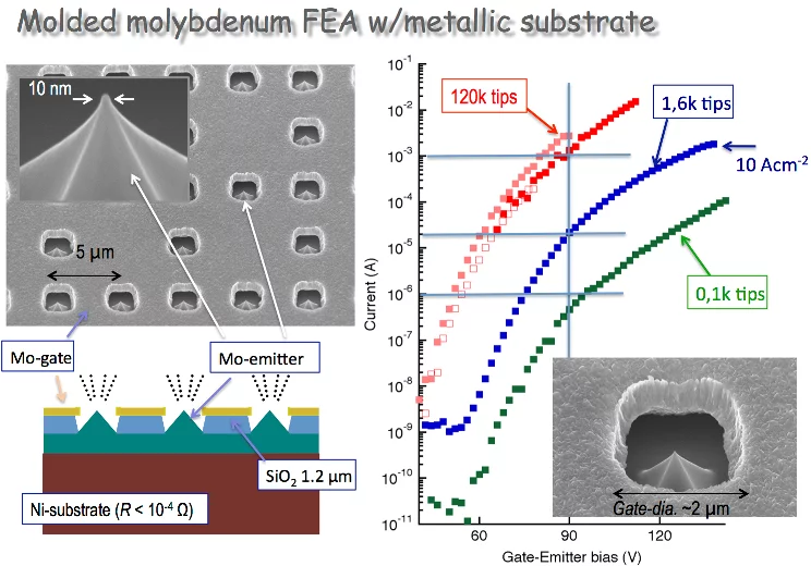
Figure 2. PSI field-emitter array cathode: overview
Unlike the celebrated Spindt FEA, first demonstrated by C.A. Spindt [1], the PSI all-metallic FEA fabrication method is based on a unique molding method [2,3] that can produce a uniform emitter-tip array over a large area. These metallic nanotips have tip apex radii of curvature in the order of a few nanometres. Single-gate and double-gate FEAs are fabricated based on the molded metallic field emitter arrays [2,3,4,5]. Development of sub-micron pitch FEAs to further increase the quantum efficiency of the laser-induced field emission is under way [6,7].
Array fabrication by molding
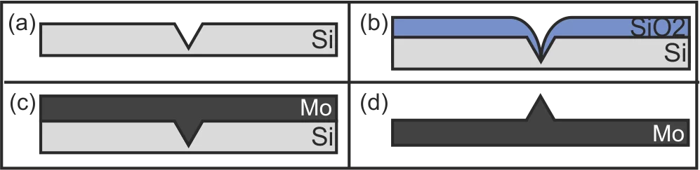
(a) directional etching of pyramidal pits into Si wafer
(b) multiple thermal oxidation steps control pit apex diameter
(c) sputter-fill mold with Molybdenum
(d) chemically remove Si wafer
(b) multiple thermal oxidation steps control pit apex diameter
(c) sputter-fill mold with Molybdenum
(d) chemically remove Si wafer
Gate fabrication: electron extraction electrode
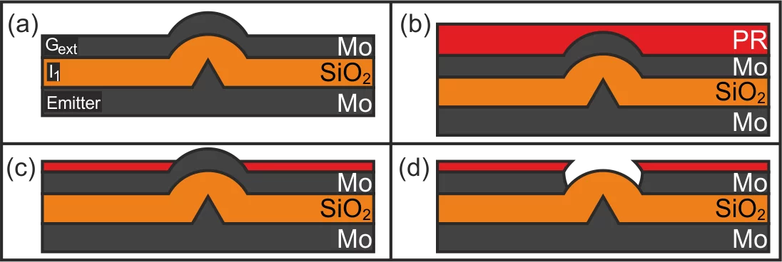
(a) deposit insulator and extraction gate electrode
(b) spin-coat photoresist (PR)
(c) thin PR in oxygen plasma to form extraction gate aperture etch mask
(d) wet-etch Molybdenum
(b) spin-coat photoresist (PR)
(c) thin PR in oxygen plasma to form extraction gate aperture etch mask
(d) wet-etch Molybdenum
Gate fabrication: electron collimation electrode
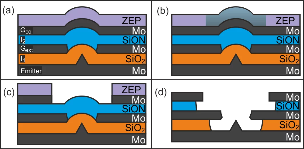
(a) deposit insulator (SiON), collimation gate electrode and ZEP resist
(b) form collimation gate aperture by selectively exposing ZEP by e-beam lithography
(c) develop ZEP and wet-etch Molybdenum
(d) remove insulator on top of tips by wet-etching
(b) form collimation gate aperture by selectively exposing ZEP by e-beam lithography
(c) develop ZEP and wet-etch Molybdenum
(d) remove insulator on top of tips by wet-etching
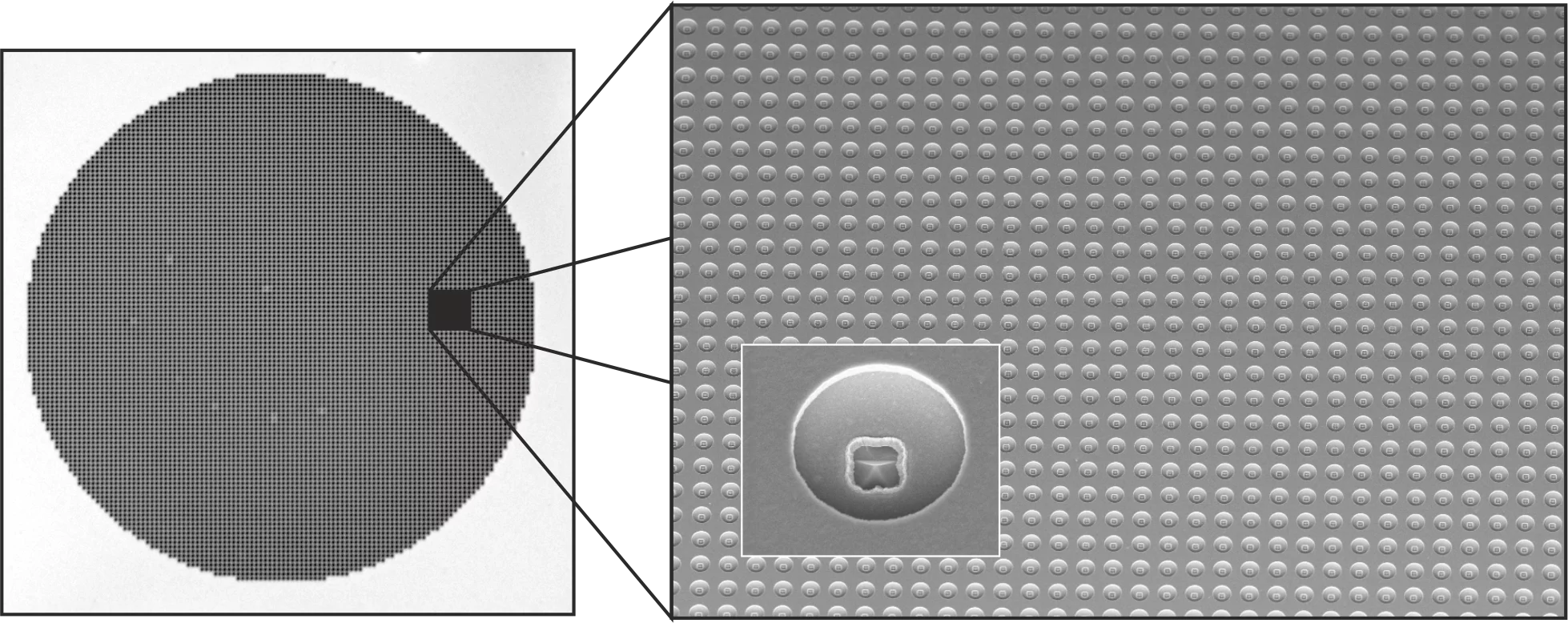
SEM images of the PSI-FEA
References
[1] C.A. Spindt, J. Appl. Phys. 39 3504 (1968).
[2] E. Kirk, S. Tsujino, T. Vogel, K. Jefimovs, J. Gobrecht, A. Wrulich, Fabrication of all-metal field emitter arrays with controlled apex sizes by molding, J. Vac. Sci. Technol. B 27, 1813 (2009).
[3] P. Helfenstein, E. Kirk, K. Jefimovs, T. Vogel, C. Escher, H.-W. Fink, and S. Tsujino, Highly collimated electron beams from double-gate field emitter arrays with large collimation gate apertures, Appl. Phys. Lett. 98, 061502 (2011).
[4] P. Helfenstein, K. Jefimovs, E. Kirk, C. Escher, H.-W. Fink, and S. Tsujino, Fabrication of metallic double-gate field emitter arrays and their electron beam collimation characteristics, J. Appl. Phys. 112, 093307 (2012).
[5] P. Helfenstein, V. A. Guzenko, H.-W. Fink, and S. Tsujino, Electron beam collimation with 40,000 tip metallic double gate field emitter arrays and in-situ control of nanotip sharpness distribution, J. Appl. Phys. 113, 043306 (2013).
[6] A. Mustonen, V. Guzenko, C. Spreu, T. Feurer, and S. Tsujino, High-density metallic nano-emitter arrays and their field emission characteristics, Nanotechnology 25, 085203 (2014).
[7] V. Guzenko, A. Mustonen, P. Helfenstein, E. Kirk, and S. Tsujino, High-density large-scale field emitter arrays for X-ray free electron laser cathodes, Microelectronic Engineering (2013).