

FIeld emission from solid surfaces generates electron beam by quantum mechanical tunneling. This can be achieved by applying an extremely strong electric field, which substantially reduces the surface potential barrier thickness. This way, one can obtain "cold" electron beam, in strong contrast to the thermionic emission, in which electrons are "evaporated" from solid by heating the material, or the photo emission, in which single or multiple photon absorption gives energy to the electron gas in the solid, and some part of those escape from the surface potential barrier, overcoming the work function.
Required electric field to generated field electron emission is extremely high, 1-5 GV/m, but can be achieved by using extremely sharp nanotips. When one of the electrode of a capacitor is replaced with such a nanotip with the tip apex radius of curvature in nanometers range, the tip apex field can be several orders of magnitude higher than the uniform field defined by the macroscopic separation between the capacitor electrode.
Required electric field to generated field electron emission is extremely high, 1-5 GV/m, but can be achieved by using extremely sharp nanotips. When one of the electrode of a capacitor is replaced with such a nanotip with the tip apex radius of curvature in nanometers range, the tip apex field can be several orders of magnitude higher than the uniform field defined by the macroscopic separation between the capacitor electrode.
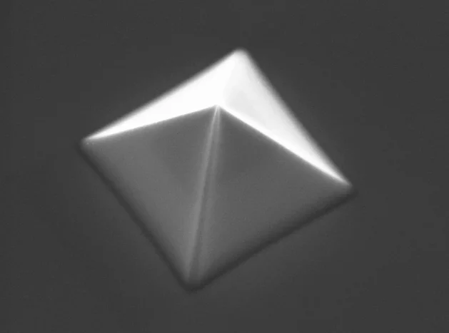
Fig.1 A metallic nanotip fabricated by molding with double-oxidation method (see Ref. 1)
In micro-fabricated field emitter arrays, with on-chip electron extraction electrode, electrons are extracted from an array of such nanotips, by applying ~100 V to the gate, to generate high current with high current density, as demonstrated with the cerebrated Spindt field emitter arrays made of molybdenum emitters. Other types of field emitter arrays include Silicon (and other semiconductor based) field emitter arrays, and carbon (carbon nanotubes, nano-diamond, graphenes) field emitter arrays.
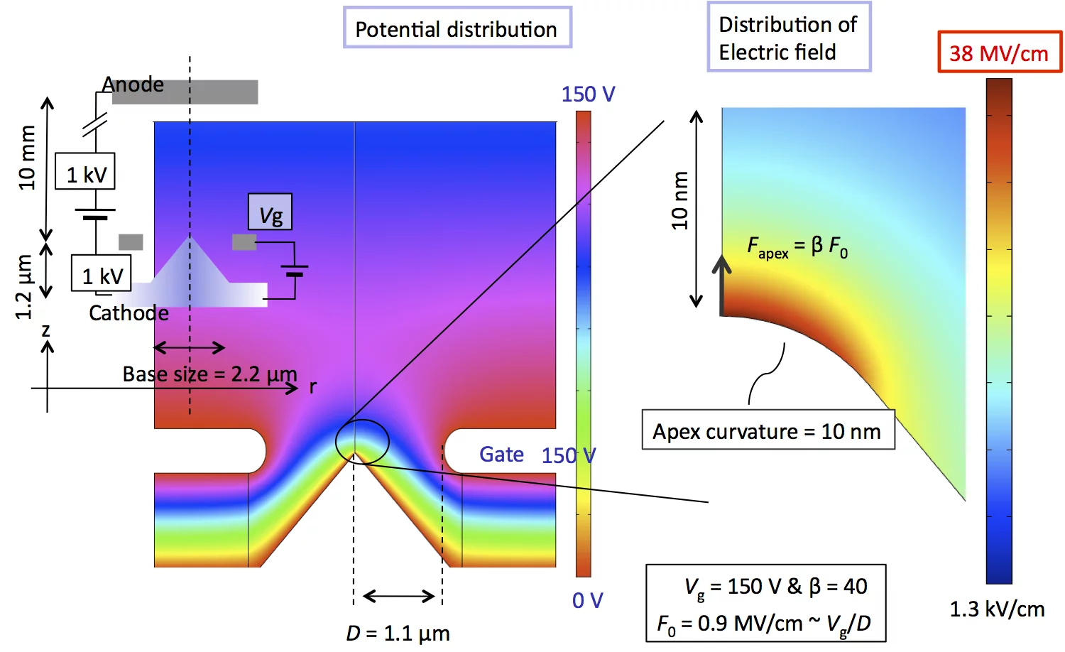
Fig.2 Single-gate emitter: potential and field-distribution
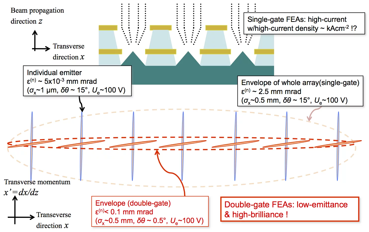
Fig.3 Phase space schematic of electron beam from field emitter arrays: substantial reduction of array beam emittance with double-gate structures
In the Laboratory of Micro- and Nanotechnology at the Paul Scherrer Institute, we fabricate all metallic field emitter arrays consisting molybdenum nanotips on metallic substrate, with an electron extraction gate electrode, as well as an on-chip electron beam collimation electrodes. Using such field emitter arrays, we demonstrated that not only static electric field but also optical electric field are concentrated locally at the sharp nanotip apexes,[2] which lead to the first demonstration of the ultrafast near infrared laser-induced emission from metallic nanotip arrays with on-chip electron extraction gate electrode.[3,4]
With the double-gate field emitter arrays, one can colliamte the individual beamlets from the emitter arrays by applying a potential to on-chip beam collimation gate electrode.[5] Combined with the high current, high current density, and laser-induced field emission, we aim at realizing a new cathode with extremely brightness.
With the double-gate field emitter arrays, one can colliamte the individual beamlets from the emitter arrays by applying a potential to on-chip beam collimation gate electrode.[5] Combined with the high current, high current density, and laser-induced field emission, we aim at realizing a new cathode with extremely brightness.
References
[1] E. Kirk, S. Tsujino, T. Vogel, K. Jefimovs, J. Gobrecht, A. Wrulich, Fabrication of all-metal field emitter arrays with controlled apex sizes by molding, J. Vac. Sci. Technol. B 27, 1813 (2009).
[2] S. Tsujino, F. le Pimpec, J. Raabe, M. Buess, M. Dehler, E. Kirk, J. Gobrecht, and A. Wrulich, Static and optical field enhancement in metallic nanotips studied by two-photon photoemission microscopy and spectroscopy excited by picosecond laser pulses, Appl. Phys. Lett. 94, 093508 (2009); Selected for the March 16, 2009 issue of Virtual Journal of Nanoscale Science & Technology; Selected for April 2009 issue (Volume 8, Issue 4) of Virtual Journal of Ultrafast Science.
[3] S. Tsujino, P. Beaud, E. Kirk, T. Vogel, H. Sehr, J. Gobrecht, and A. Wrulich Ultrafast electron emission from metallic nanotip arrays induced by near infrared femtosecond laser pulses, Appl. Phys. Lett. 92, 193501 (2008); Selected in Virtual Journal of Ultrafast Science -- June 2008, Volume 7, Issue 6.
[4] A. Mustonen, P. Beaud, E. Kirk, T. Feurer, and S. Tsujino, Five picocoulomb electron bunch generation by ultrafast laser-induced field emission from metallic nano-tip arrays, Appl. Phys. Lett. 99, 103504 (2011); Selected for September 19, 2011 issue (Volume 24, Issue 12) of Virtual Journal of Nanoscale Science & Technology; Selected for October 2011 issue (Volume 10, Issue 10) of Virtual Journal of Ultrafast Science; highlighted in Nature Photonics, 5, 644-645 (November 2011).
[5] P. Helfenstein, E. Kirk, K. Jefimovs, T. Vogel, C. Escher, H.-W. Fink, and S. Tsujino, Highly collimated electron beams from double-gate field emitter arrays with large collimation gate apertures, Appl. Phys. Lett. 98, 061502 (2011).