Recognition at MNE 2024 Micrograph Contest
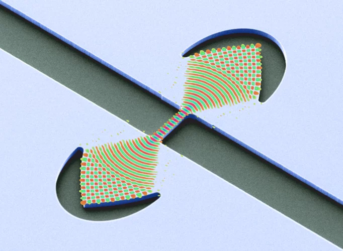
The MNE conference is the flagship event of the International Society for Micro- and Nanotechnology (iMNEs). The research fields covered by the MNE conferences have consistently driven advancements in the development of smaller and smaller structures. To emphasize the significance of micrographs in this field, the conference features a micrograph contest, sponsored and hosted by Zyvex Labs. Entries are judged based on both their technological relevance and artistic merit.
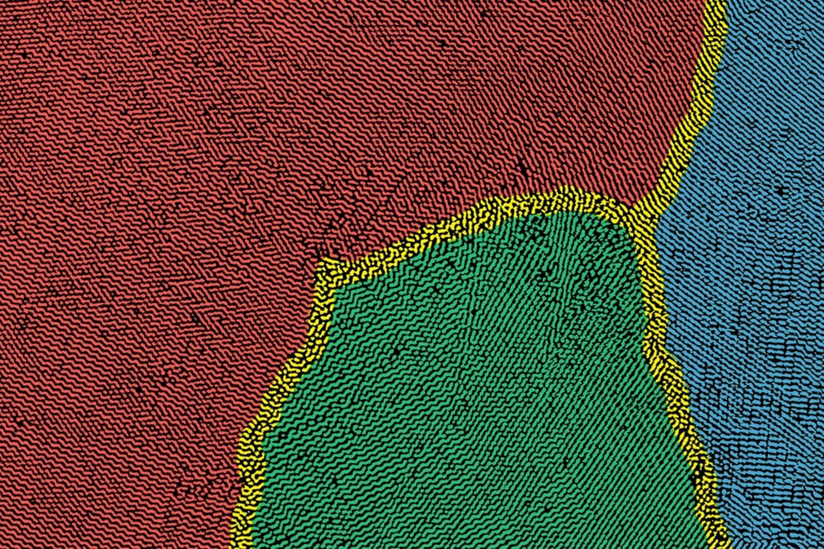
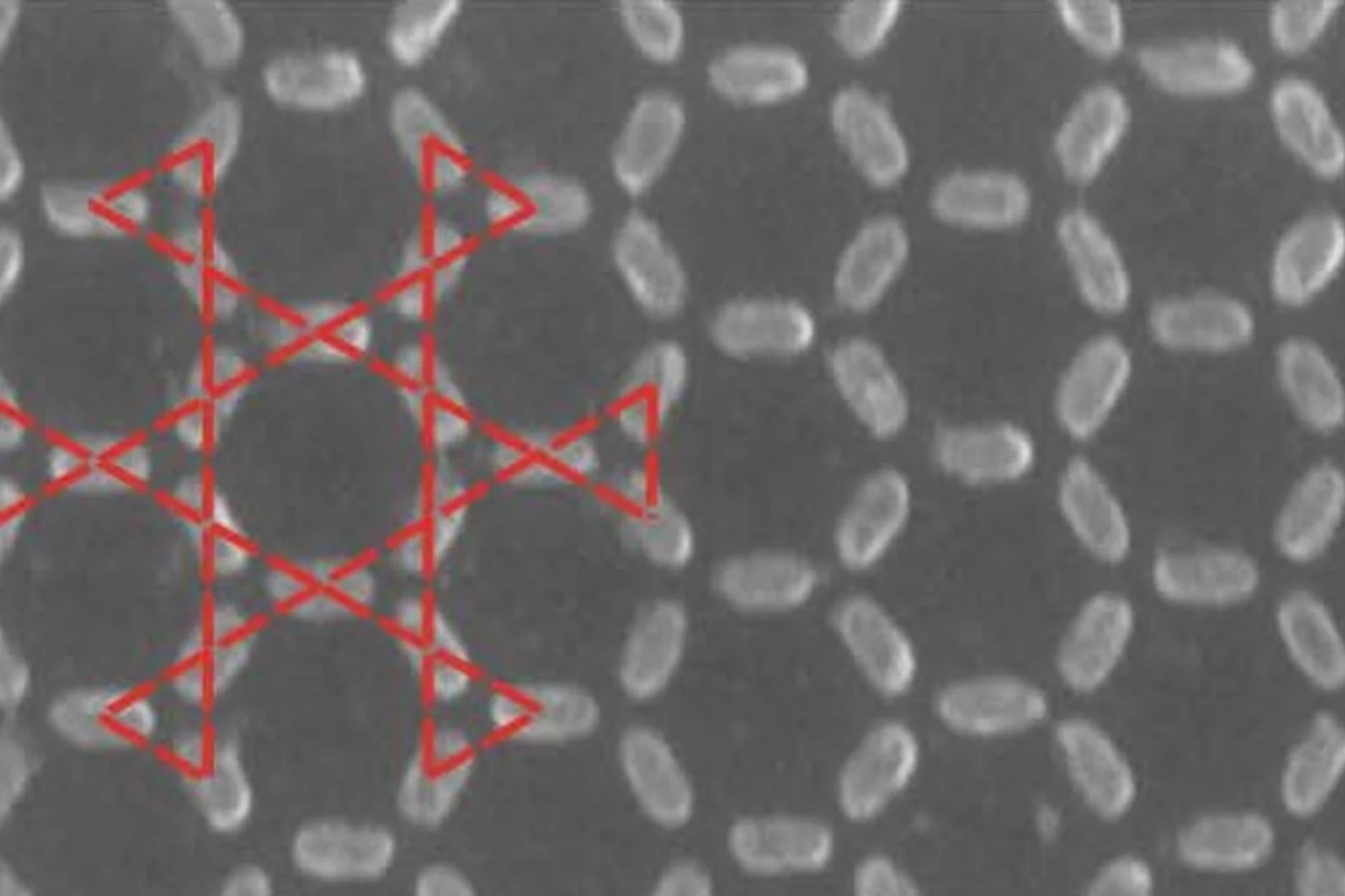
This year, Peng Qi from the X-ray Nano Optics group, LXN, CPS, earned third place and an honorable mention for his two submitted images.
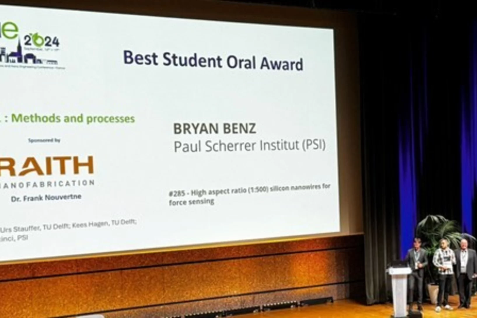
Bryan Benz awarded best talk at MNE 2024
Bryan Benz was awarded the conference’s best oral presentation at the 50th International Micro and Nano Engineering Conference (MNE 2024) for his talk entitled “High aspect ratio (1:500) silicon nanowires for force sensing”.
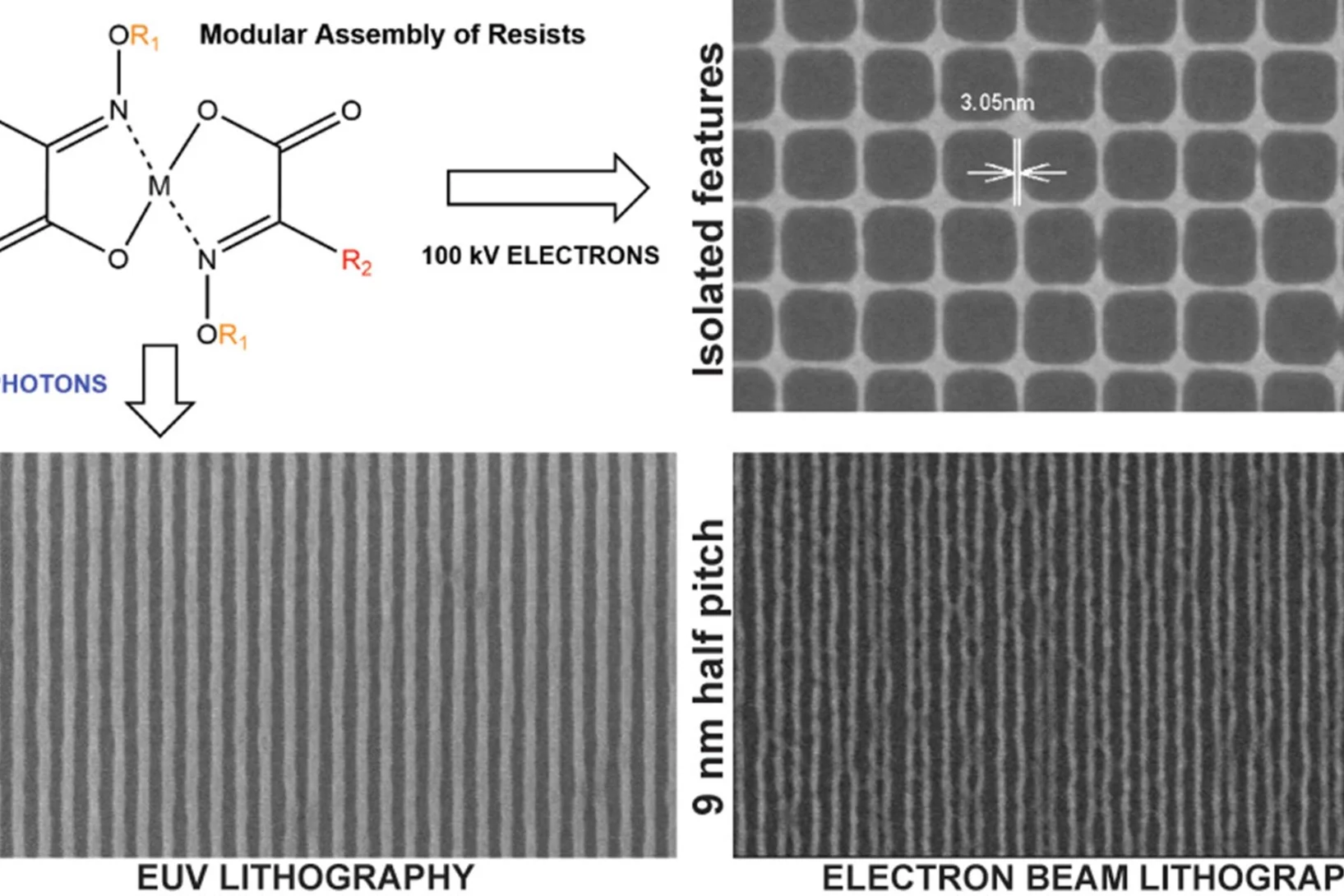
Novel Photoresist Chemistry Enables Lithography Approaching Angstrom-Scale Resolution
Photoresist materials are crucial in the manufacturing of computer chips, where the circuits are initially printed in the photoresist using photolithography. As the demand for smaller and more precise circuitry in computer chips grows, photoresists must resolve features with smaller sizes and higher density. One of the factors determining the ultimate resolution in lithography is the molecular size/mass of the photoresists.
Researchers show that computer chips have the potential to become even smaller
Researchers at PSI reach unprecedented 5 nanometres half pitch resolution with EUV lithography.
New X-ray world record: Looking inside a microchip with 4 nanometre precision
Researchers at PSI have succeeded in imaging the spatial structure of a computer chip with a record resolution of 4 nanometres using X-rays.
Nanoimaging Reveals Topological Textures in Nanoscale Crystalline Networks
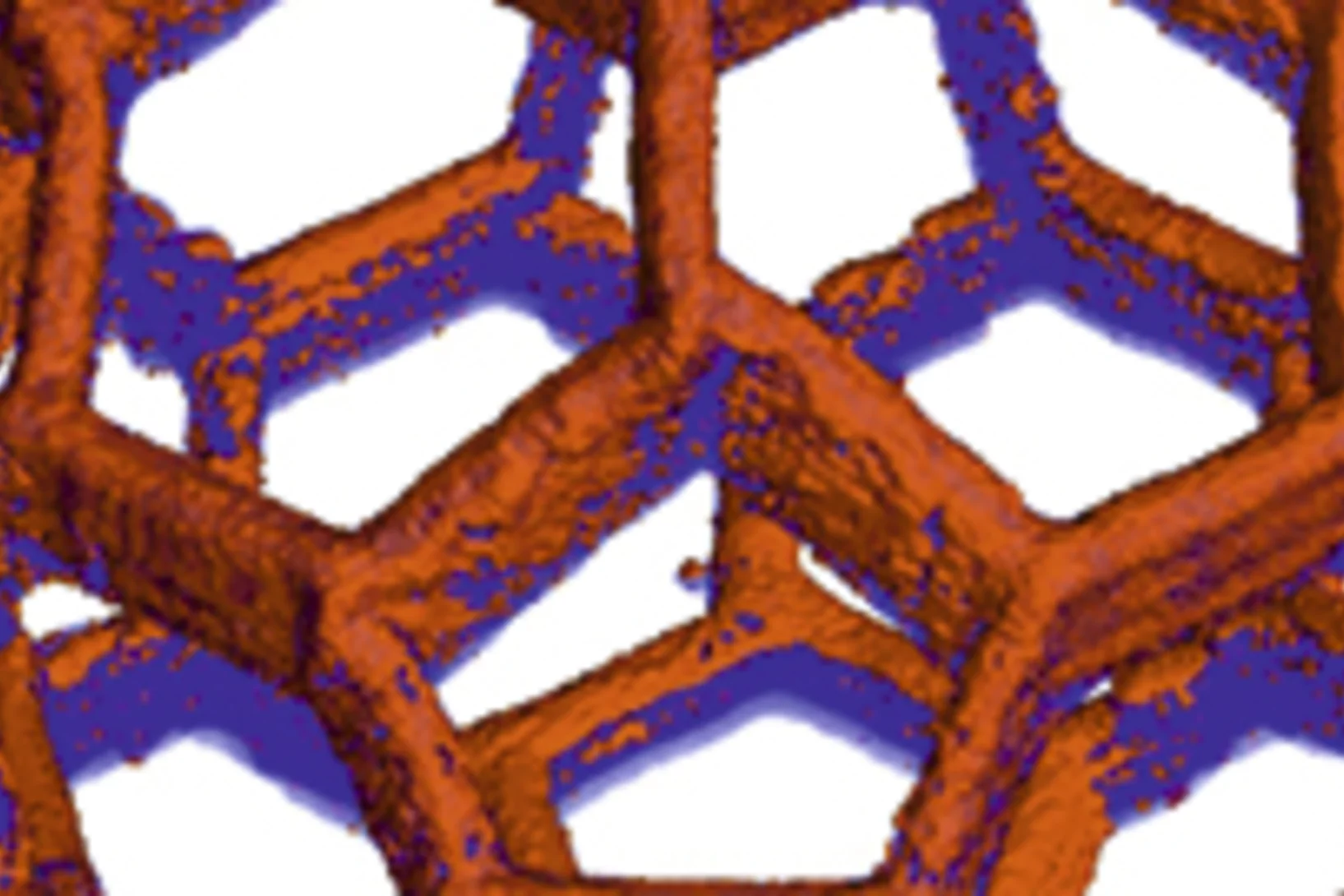
X-ray nano-tomography reveals collective behavior in synthetic self-assembled nanostructures. The new method opens opportunities for the synthesis of photonic and plasmonic materials with improved long-range ordering.
PSI-UCL-Surrey workshop on silicon and germanium based quantum devices
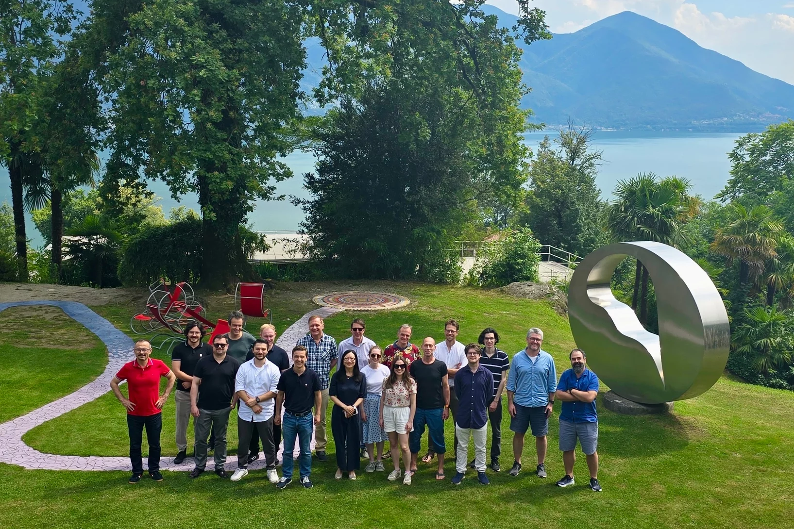
A team of PSI scientists as well as collaborators from UCL and the University of Surrey met at the Fondazione Monte Verità to discuss results and trace the roadmap for future research into quantum devices based on silicon and germanium.
New process for the production of semiconductors
The Paul Scherrer Institute PSI and the Finnish company PiBond to collaborate in the commercialization of advanced EUV semiconductor lithography products.
Swiss Quantum Days Poster Prize for Adrian Rutschmann
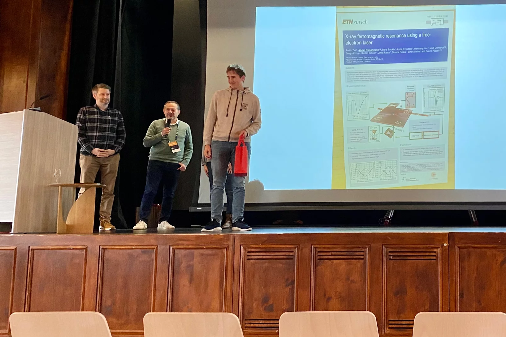
Congratulations Adrian Rutschmann for winning a prize at the Swiss Quantum Days 2024 for a poster on our recent X-ray-detected ferromagnetic resonance experiment at SwissFEL.
“Molecular chains could be useful for the electronics of the future”
Christian Wäckerlin talks about fundamental research into novel nanowires and their potential applications.
PSI researchers use extreme UV light to produce tiny structures for information technology.
Synchrotron light can be used in follow-up after a heart transplant to determine whether the body may be rejecting the new organ.
“If you’re in a certain position, you should step forward”
Kirsten Moselund heads the new Laboratory for Nano and Quantum Technologies. In this interview she discusses quantum research at PSI and how nanophotonics can assist with this.
Scientists develop a new kind of qubit based on the concept of Schrödinger’s cat
Scientists in the Applied Physics department of Yale University – one of the leading authors, Alexander Grimm, has in the meantime relocated to PSI – have developed a new device that combines the Schrödinger’s cat concept of superposition (a physical system existing in two states at once) with the ability to fix some of the trickiest errors in a quantum computation.
To the sun and beyond
PSI takes part in space research projects. This not only expands knowledge about our astronomical home, but also reinforces Switzerland's reputation as a reliable developer of sophisticated space equipment.
First demonstration of a Germanium laser
Scientist at the Paul Scherrer Institut and ETH Zürich, with colleagues from CEA Grenoble, have demonstrated and characterized a technology that, for the first time, yields lasing from strained elemental Germanium. This achievement underlines PSI’s leading role in the development of Silicon-compatible laser light sources.
Watching electrons and switching bits on
Electronics should get smaller, faster, and above all more energy-efficient. These themes are also present in several research groups at PSI. From incremental improvements to complete rethinking – who is currently working on what?
Power from nanomagnets
Oles Sendetskyi, winner of a Founder Fellowship at the Paul Scherrer Institute PSI, wants to use polarity reversal in nanomagnets to develop a sustainable power source for small devices.
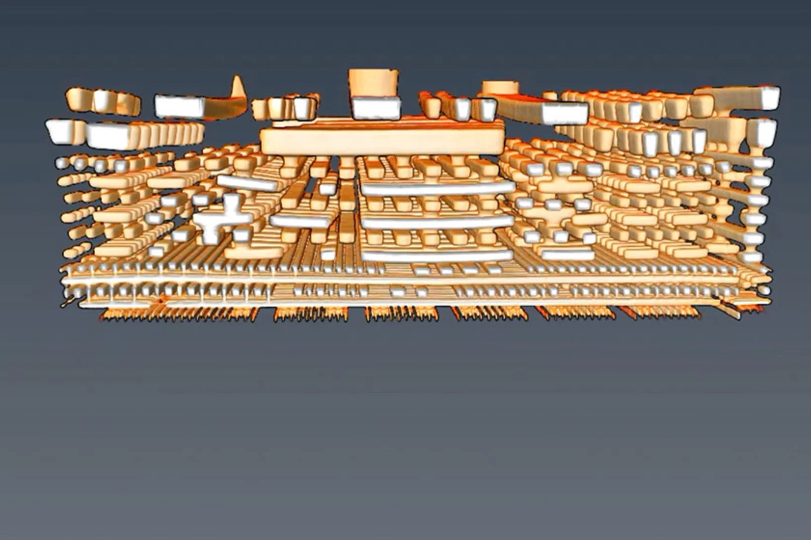
3-D X-ray imaging makes the finest details of a computer chip visible
Researchers at the PSI have made detailed 3-D X-ray images of a commercially available computer chip. In their experiment, they examined a small piece that they had cut out of the chip beforehand. This sample remained undamaged throughout the measurement. It is a major challenge for manufacturers to determine if, in the end, the structure of their chips conforms to the specifications. Thus these results represent one important application of an X-ray tomography method that the PSI researchers have been developing for several years.
Nanotechnology enables new insights into chemical reactions
Eighty percent of all products of the chemical industry are manufactured with catalytic processes. Catalysis is also indispensable in energy conversion and treatment of exhaust gases. Industry is always testing new substances and arrangements that could lead to new and better catalytic processes. Researchers of the Paul Scherrer Institute PSI in Villigen and ETH Zurich have now developed a method for improving the precision of such experiments, which may speed up the search for optimal solutions.
A micrometer-sized model of the Matterhorn
Researchers at the Paul Scherrer Institute have produced large numbers of detailed models of the Matterhorn, each one less than a tenth of a millimetre in size. With this, they demonstrated how 3-D objects so delicate could be mass-produced. Materials whose surface is covered with a pattern of such tiny 3-D structures often have special properties, which could for example help to reduce the wear and tear of machine parts.
Tiny magnets mimic steam, water and ice
Researchers at the Paul Scherrer Institute (PSI) created a synthetic material out of 1 billion tiny magnets. Astonishingly, it now appears that the magnetic properties of this so-called metamaterial change with the temperature, so that it can take on different states; just like water has a gaseous, liquid and a solid state.
Seven nanometres for the electronics of the future
Researchers from the Paul Scherrer Institute have succeeded in creating regular patterns in a semiconductor material that are sixteen times smaller than in today’s computer chips. As a result, they have taken an important step closer towards even smaller computer components. Industry envisages structures on this scale as the standard for the year 2028.
Research geared towards the future
Interview with Gabriel AeppliGabriel Aeppli has been head of synchrotron radiation and nanotechnology research at PSI since 2014. Previously, the Swiss-born scientist set up a leading research centre for nanotechnology in London. In this interview, Aeppli explains how the research approaches of the future can be implemented at PSI's large research facilities and talks about his view of Switzerland.
Split x-ray flash shows rapid processes
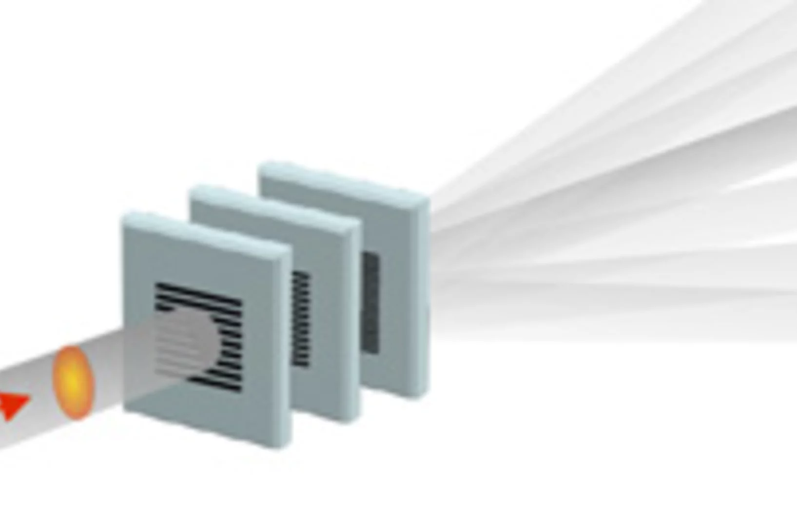
SwissFEL, PSI’s x-ray laser, is to render the individual steps of very rapid processes visible. A new method will facilitate especially precise experiments: the individual x-ray flashes are split into several parts that arrive at the object under examination one by one. The principle of the method harks back to the ideas of the earliest high-speed photography.
Nanometres in 3D
Scientists at the Paul Scherrer Institute and ETH Zurich have created 3D images of tiny objects showing details down to 25 nanometres. In addition to the shape, the scientists determined how particular chemical elements were distributed in their sample and whether these elements were in a chemical compound or in their pure state.
New laser for computer chips
Germanium-Zinn-Halbleiterlaser lässt sich direkt auf Siliziumchips aufbringenWinzige Laser, die in Computerchips aus Silizium eingebaut werden, sollen in Zukunft die Kommunikation innerhalb der Chips und zwischen verschiedenen Bauteilen eines Computers beschleunigen. Lange suchten Experten nach einem dafür geeigneten Lasermaterial, das sich mit dem Fertigungsprozess von Siliziumchips vereinbaren lässt. Wissenschaftler des Forschungszentrums Jülich und des Paul Scherrer Instituts PSI haben hier nun einen wichtigen Fortschritt erzielt.This news release is only available in German.
The cleanest place at the Paul Scherrer Institute
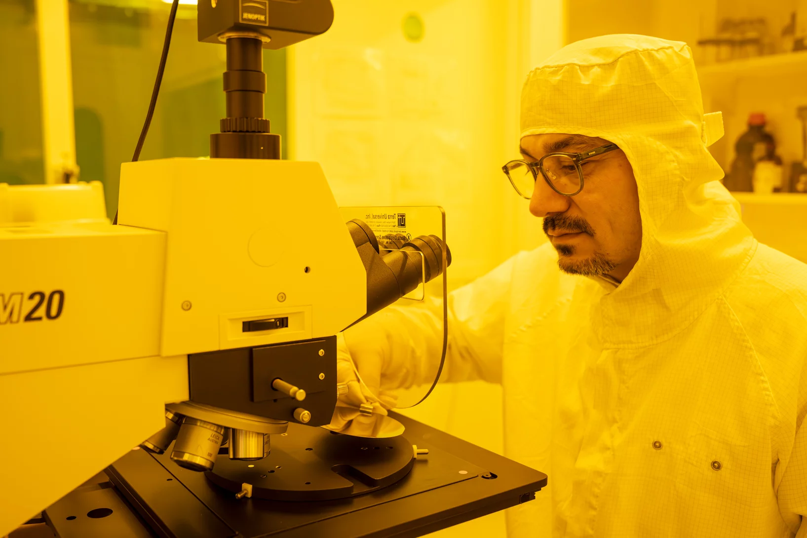
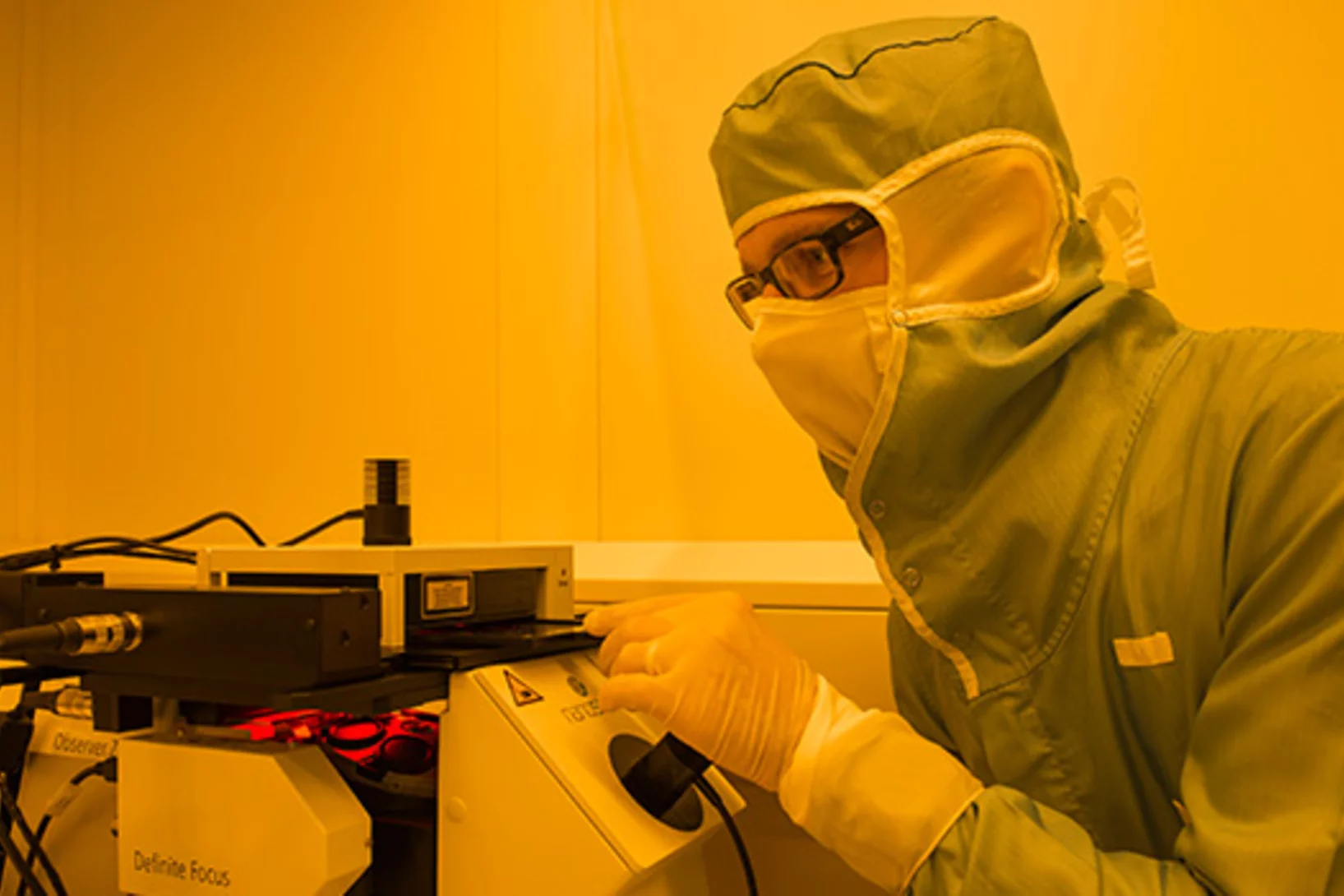
Highly sensitive processes take place in the cleanrooms of the Paul Scherrer Institute (PSI) as a single dust particle in the wrong place could have disastrous consequences. Here is a glimpse behind the scenes in rooms that are so clean even pencils are prohibited.
Germanium – zum Leuchten gezogen
Forscher des PSI und der ETH Zürich haben mit Kollegen vom Politecnico di Milano in der aktuellen Ausgabe der wissenschaftlichen Fachzeitschrift "Nature Photonics" eine Methode erarbeitet, einen Laser zu entwickeln, der schon bald in den neuesten Computern eingesetzt werden könnte. Damit könnte die Geschwindigkeit, mit der einzelne Prozessorkerne im Chip miteinander kommunizieren, drastisch erhöht werden. So würde die Leistung der Rechner weiter steigen.This news release is only available in German.
Magnetic nano-chessboard puts itself together
Researchers from the Paul Scherrer Institute and the Indian Institute of Science Education and Research have been able to intentionally switch off’ the magnetization of every second molecule in an array of magnetized molecules and thereby create a magnetic nano-chessboard’. To achieve this, they manipulated the quantum state of a part of the molecules in a specific way.
Silicon – Close to the Breaking Point
Stretching a layer of silicon can lead to internal mechanical strain which can considerably improve the electronic properties of the material. Researchers at the Paul Scherrer Institute and the ETH Zurich have created a new process from a layer of silicon to fabricate extremely highly strained nanowires in a silicon substrate. The researchers report the highest-ever mechanical stress obtained in a material that can serve as the basis for electronic components. The long term goal aim is to produce high-performance and low-power transistors for microprocessors based on such wires.
